Best Practices for Thickening Power Traces in PCB Design
Introduction
In printed circuit board (PCB) design, power delivery is a critical aspect that directly impacts the performance, reliability, and efficiency of electronic devices. Power traces must be designed to handle the required current without excessive voltage drop, overheating, or signal integrity issues. One of the most effective ways to ensure robust power distribution is by appropriately thickening power traces. This article explores the key considerations, calculation methods, and design techniques for optimizing power trace width in PCB layouts.
Why Thicken Power Traces?
Power traces carry higher currents than signal traces, and inadequate trace width can lead to several problems:
- Excessive Resistance – Thin traces have higher resistance, leading to voltage drops (Ohm’s Law: V = I × R).
- Heat Generation – High current in narrow traces increases power dissipation (P = I² × R), causing overheating.
- Reduced Efficiency – Voltage drops degrade power supply performance, affecting sensitive components.
- Potential Failure – Sustained overheating can damage traces or delaminate the PCB.
To mitigate these issues, designers must calculate and implement appropriate trace widths based on current requirements, copper weight, and thermal considerations.
Key Factors in Determining Power Trace Width
1. Current Carrying Capacity
The width of a power trace depends primarily on the current it must carry. IPC-2221 standards provide guidelines for trace width based on:
- Current (I) – The maximum expected current.
- Copper Thickness (oz/ft²) – Common values are 0.5 oz, 1 oz, and 2 oz (1 oz = 35 µm).
- Temperature Rise (ΔT) – Acceptable temperature increase (typically 10°C, 20°C, or higher).
Several online calculators (such as Saturn PCB Toolkit) use IPC formulas to recommend trace widths.
2. Voltage Drop Considerations
Even if a trace can handle the current, excessive voltage drop may still be problematic. The acceptable drop depends on the application (e.g., digital ICs typically tolerate ~5% drop, while analog circuits may need tighter regulation).
The voltage drop can be estimated using:
[
\Delta V = I \times R_{trace}
]
where ( R_{trace} ) is the trace resistance, calculated as:
[
R_{trace} = \rho \times \frac{L}{A}
]
- ( \rho ) = Copper resistivity (~1.7×10⁻⁶ Ω·cm)
- ( L ) = Trace length
- ( A ) = Cross-sectional area (width × thickness)
If the drop is too high, increasing trace width or using thicker copper is necessary.
3. Thermal Management
High-current traces generate heat, which must be dissipated to prevent damage. Techniques include:
- Wider Traces – Lower resistance reduces heat generation.
- Copper Pours – Large filled areas improve heat dissipation.
- Thermal Reliefs – Used when connecting to pads to ease soldering while maintaining conductivity.
4. PCB Layer Stackup
Multilayer PCBs often dedicate entire layers to power planes, which offer minimal resistance and inductance compared to traces. If thick traces are still needed, consider:
- Inner Layers – May require wider traces due to less efficient heat dissipation.
- External Layers – Can dissipate heat better, allowing slightly thinner traces.
Practical Methods to Thicken Power Traces
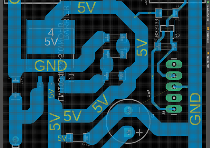
1. Manual Trace Width Adjustment
Most PCB design tools (Altium, KiCad, Eagle) allow manual width settings. Steps include:
- Identify high-current paths (e.g., from voltage regulators to ICs).
- Set custom widths (e.g., 20-50 mil for moderate current, 100+ mil for high current).
- Avoid sharp corners; use curved or 45° bends to reduce current crowding.
2. Using Copper Pours (Power Planes)
For very high currents, replace traces with copper pours:
- Create a polygon pour connected to the power net.
- Ensure sufficient clearance from other signals.
- Use multiple vias for connections to reduce impedance.
3. Multiple Parallel Traces
If a single wide trace is impractical (due to space constraints), use multiple parallel traces on different layers, connected with vias. This distributes current and reduces effective resistance.
4. Increasing Copper Weight
Standard PCBs use 1 oz copper, but high-power designs may require 2 oz or thicker copper. This allows narrower traces for the same current but increases cost.
5. External Bus Bars or Wire Jumpers
For extremely high currents (e.g., >10A), consider:
- Soldering thick wires over PCB traces.
- Using bus bars (metal strips) for power distribution.
Design Example
Scenario: A 5V power trace carrying 3A with 1 oz copper and a max 10°C temperature rise.
- Calculate Required Width:
Using IPC-2221 charts or an online calculator, a 3A current with 1 oz copper requires ~120 mil width for 10°C rise. - Check Voltage Drop:
For a 5-inch trace:
[
R_{trace} = 1.7 \times 10^{-6} \times \frac{5 \times 2.54}{0.12 \times 0.0035} \approx 0.016 \, \Omega
]
[
\Delta V = 3 \times 0.016 = 0.048V \, (<1\%, acceptable)
] - Implement in PCB Layout:
- Route a 120 mil trace or use a copper pour.
- Add multiple vias if transitioning layers.
Conclusion
Thickening power traces is essential for maintaining voltage integrity, minimizing heat, and ensuring reliability in PCB designs. By considering current requirements, copper weight, thermal factors, and using appropriate layout techniques (wide traces, pours, parallel paths), designers can optimize power delivery efficiently. Always verify designs with calculations and simulation tools to prevent power-related failures.
By following these best practices, engineers can create robust PCBs capable of handling high currents while maintaining performance and longevity.