Best Practices for VCC and Ground Handling in PCB Design
Introduction
Proper handling of power (VCC) and ground connections is one of the most critical aspects of printed circuit board (PCB) design that directly impacts the performance, reliability, and electromagnetic compatibility (EMC) of electronic systems. This article provides a comprehensive guide to managing VCC and ground in PCB layouts, covering fundamental principles, routing strategies, layer stackup considerations, and advanced techniques for optimal power distribution.
1. Fundamental Principles of Power Distribution
1.1 Understanding Current Return Paths
Every signal current traveling through a trace requires a return path, which typically flows through the ground system. The fundamental rule of power distribution states that current always takes the path of least impedance (not just resistance), which becomes particularly important at high frequencies where inductive reactance dominates.
1.2 The Importance of Low Impedance Power Delivery
A well-designed power distribution network (PDN) must provide:
- Low DC resistance to minimize voltage drops
- Low AC impedance to handle transient currents
- Adequate current-carrying capacity for all components
- Minimal loop areas to reduce electromagnetic interference (EMI)
1.3 Power Integrity Considerations
Modern high-speed designs require careful attention to power integrity (PI), which involves:
- Maintaining stable voltage levels despite current fluctuations
- Minimizing simultaneous switching noise (SSN)
- Controlling ground bounce effects
- Managing power plane resonances
2. PCB Stackup Design for Optimal Power Distribution
2.1 Multilayer Board Considerations
For most modern designs, a 4-layer or more stackup is recommended:
- Signal
- Ground plane (solid)
- Power plane (can be split for multiple voltages)
- Signal
Additional layers in high-density designs should maintain alternating power/ground planes when possible.
2.2 Plane Capacitance Benefits
Adjacent power and ground planes create natural decoupling capacitance:
- FR4 dielectric (εr≈4.3) provides about 100pF/in²
- Thinner dielectrics increase this capacitance
- This distributed capacitance helps filter high-frequency noise
2.3 Layer Pairing Strategies
Follow these guidelines for layer pairing:
- Route high-speed signals adjacent to solid reference planes
- Pair each power plane with an adjacent ground plane
- Maintain symmetry in the stackup to prevent warping
3. VCC Routing Techniques
3.1 Power Plane Usage
For primary system voltages (like 3.3V, 5V), use dedicated power planes when possible:
- Provides lowest impedance path
- Offers excellent current distribution
- Minimizes voltage drops
- Reduces electromagnetic radiation
3.2 Power Trace Design
When planes aren’t available or for secondary voltages:
- Calculate required trace width based on current (use IPC-2152 standards)
- Use thicker copper (2oz or more) for high-current paths
- Implement star routing for sensitive analog supplies
- Avoid daisy-chaining power between multiple ICs
3.3 Split Plane Considerations
When splitting power planes:
- Maintain adequate clearance (typically 0.5mm minimum)
- Avoid creating slots that block current flow
- Consider the return current paths when splitting
- Use stitching capacitors when signals cross split planes
4. Ground System Design
4.1 Ground Plane Implementation
A solid ground plane is ideal because it:
- Provides low-impedance return paths
- Reduces ground bounce
- Minimizes loop areas
- Acts as a shield against EMI
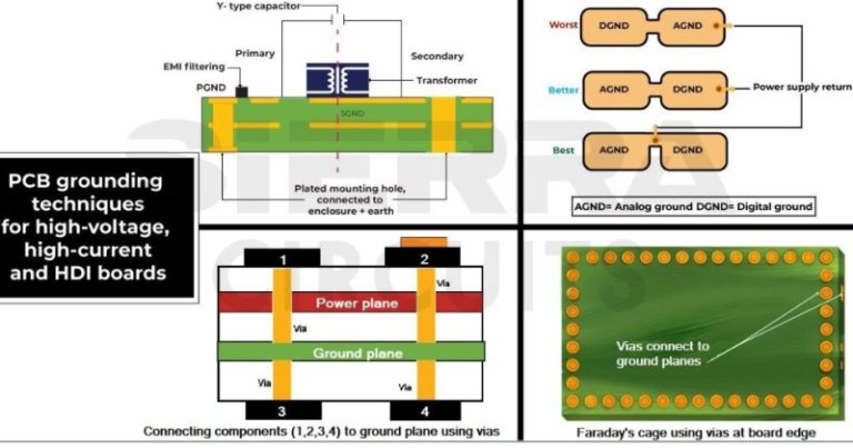
4.2 Grounding Strategies
Choose appropriate grounding approach based on application:
- Single-point grounding: Best for low-frequency analog systems
- Multi-point grounding: Required for high-speed digital systems
- Hybrid grounding: Combines both with isolation techniques
4.3 Mixed-Signal Grounding
For mixed-signal designs:
- Partition ground planes only when necessary
- Maintain single reference potential
- Route sensitive analog traces over continuous ground
- Use strategic placement of split planes if separation is required
5. Decoupling Capacitor Implementation
5.1 Decoupling Capacitor Selection
Implement a mix of capacitor values:
- Bulk capacitors (10-100μF) for low-frequency decoupling
- Medium value (0.1μF) for mid-range frequencies
- Small ceramics (0.01μF or smaller) for high frequencies
5.2 Placement Guidelines
Optimal decoupling capacitor placement:
- Place smallest value capacitors closest to IC power pins
- Connect directly to power plane with minimal via distance
- Use multiple vias for lower inductance in high-current designs
- Follow manufacturer recommendations for BGA packages
5.3 Advanced Decoupling Techniques
For high-performance designs:
- Use embedded capacitance materials
- Implement discrete capacitors on package substrates
- Consider interdigitated capacitor (IDC) structures
- Utilize die-side capacitors for very high-speed devices
6. Via Management in Power Distribution
6.1 Via Current Capacity
Understand via current limitations:
- A standard 0.3mm via can handle about 1A
- Use multiple vias in parallel for high-current paths
- Consider via diameter and plating thickness
6.2 Power Via Placement
Optimize via placement:
- Cluster vias near component power pins
- Use array vias for BGA power connections
- Balance via distribution across power planes
- Avoid creating antipads that block current flow
6.3 Via Stitching
Improve plane connectivity with via stitching:
- Place stitching vias around plane perimeters
- Use regular patterns in large plane areas
- Stitch ground planes at high-frequency intervals (λ/20 rule)
7. Special Considerations for Different Circuit Types
7.1 High-Speed Digital Circuits
- Maintain uninterrupted reference planes
- Minimize power plane discontinuities
- Implement comprehensive decoupling
- Control impedance of power delivery paths
7.2 RF and Microwave Circuits
- Use distributed decoupling approaches
- Implement quarter-wave stubs for filtering
- Consider coplanar waveguide structures
- Pay special attention to ground via placement
7.3 High-Power Applications
- Calculate adequate copper weight
- Implement thermal reliefs wisely
- Consider bus bar integration
- Monitor voltage drop across the board
7.4 Sensitive Analog Circuits
- Implement guard rings when needed
- Use separate power supplies for critical stages
- Maintain clean reference grounds
- Avoid ground loops in measurement circuits
8. Verification and Testing
8.1 Design Rule Checks (DRC)
Implement specific power-related DRCs:
- Minimum width for power traces
- Adequate via count for current needs
- Proper clearance around high-voltage traces
- Decoupling capacitor placement rules
8.2 Power Integrity Analysis
Perform simulations when possible:
- DC analysis for voltage drops
- AC analysis for impedance profiles
- Transient analysis for current demands
- Resonant mode analysis for plane behavior
8.3 Measurement Techniques
Verify designs with:
- Impedance measurements with VNA
- Ground bounce measurements
- Power rail ripple measurements
- Thermal imaging under load
9. Advanced Techniques
9.1 Power Delivery Network (PDN) Optimization
- Target impedance calculations
- Frequency-domain analysis
- Distributed decoupling networks
- On-package power solutions
9.2 Electromagnetic Bandgap (EBG) Structures
For advanced EMI control:
- Implement high-impedance surfaces
- Create artificial magnetic conductors
- Design planar EBG structures
9.3 3D Power Distribution
For multilayer HDI boards:
- Use buried capacitance materials
- Implement through-silicon vias (TSVs) in 3D ICs
- Consider interposer-based power delivery
Conclusion
Effective handling of VCC and ground in PCB design requires careful consideration of both fundamental principles and application-specific requirements. By implementing proper stackup design, strategic component placement, optimized routing techniques, and thorough verification methods, designers can create power distribution systems that meet the demanding requirements of modern electronic circuits. As power requirements continue to evolve with advancing technology, staying informed about new materials, design methodologies