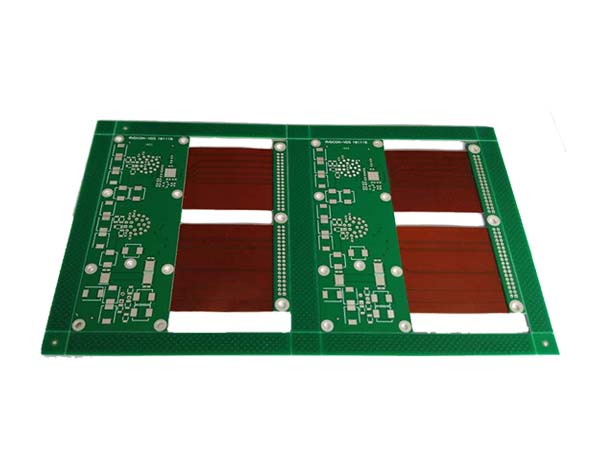
Beta layout flex pcb
A beta layout flex PCB is a type of printed circuit board that is designed to be flexible and bendable.
It is typically used in applications where a rigid PCB would not be suitable,
such as in wearable technology, medical devices, and other applications where space is limited.
The layout of a beta layout flex PCB is designed to allow for the board to be bent and flexed without damaging the circuitry.
This is achieved by using flexible materials such as polyimide or polyester film, which are layered with conductive traces and other components.
The beta layout flex PCB is typically designed using specialized software that allows for the creation of flexible circuitry.
The layout is then printed onto the flexible material using a specialized printer, and the components are added using a pick-and-place machine.
Once the beta layout flex PCB is completed, it can be tested to ensure that it meets the required specifications.
This may involve testing for electrical conductivity, resistance, and other factors that are important for the intended application.
Overall, the beta layout flex PCB is a versatile and flexible solution for a wide range of applications,
and it is becoming increasingly popular as technology continues to evolve.

where is the beta layout flex pcb used?
Beta layout flex PCBs are used in a wide range of applications, including consumer electronics, medical devices,
automotive electronics, aerospace, and military applications.
They are commonly used in devices that require flexible and lightweight circuitry,
such as wearable technology, mobile phones, tablets, and laptops.
Beta layout flex PCBs are also used in high-density interconnect (HDI) applications, where space is limited and multiple layers of circuitry are required.
Flex PCB Use Cases
Actually the examples of using flex PCB is unlimited,
but showing some could clarify the importance of this technology rather than thinking that it is only good for connectors and screen panels.
Regards using flex PCB as connectors, it could be a cost effective approach compared to rigid ones connected with wires.
This is because connecting 2 PCBs together may require in some cases designing a special harness cable or connector which will add additional steps in assembly and introduce more cost for testing and assembly.
Another case of using flex PCB is when doing a replacement of a part with a different package without changing the PCB design.

If you want to have more flexibility, then you would use thinner copper traces to have less resistance to bending.
In the same time you may use wide endings at the edge to allow soldering the flex cable somewhere else.
If the transaction is done in a sharp way then this will be considered as a weak point when soldering.
So it is better to do a gradient change in width between thin and wide traces in the mentioned case.