Blind Via PCB: Design, Manufacturing, and Applications
Abstract
This comprehensive article explores blind via PCB technology, a critical advancement in modern printed circuit board design. We examine the definition and characteristics of blind vias, compare them with other via types, and detail their manufacturing processes. The discussion covers design considerations, advantages, limitations, and various applications across industries. Current technological trends and future developments in blind via PCB technology are also analyzed, providing engineers and designers with essential knowledge for implementing this important interconnect solution.
1. Introduction to Blind Via Technology
1.1 Definition and Basic Concept
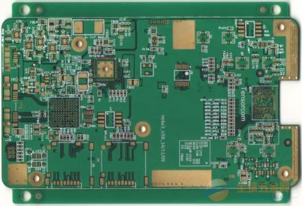
Blind vias are a specialized type of interconnect structure in printed circuit boards (PCBs) that connect an outer layer of the board to one or more inner layers without penetrating the entire board thickness. Unlike through-hole vias that pass completely through the PCB, blind vias are “blind” to the opposite side of the board, hence their name.
These microvias typically appear as small, laser-drilled holes visible on one surface of the PCB but not on the opposite side. Their diameter usually ranges from 50 to 150 microns (0.002″ to 0.006″), significantly smaller than conventional through vias. The aspect ratio (depth to diameter) of blind vias generally stays below 1:1 to ensure reliable plating, though advanced processes can achieve higher ratios.
1.2 Historical Development
The development of blind via technology emerged in the 1990s as a response to the increasing complexity of electronic devices and the need for higher density interconnections. Japanese PCB manufacturers pioneered many early blind via processes to accommodate the miniaturization demands of consumer electronics. The technology gained widespread adoption with the introduction of high-density interconnect (HDI) standards and has since become essential for modern multilayer PCB designs.
1.3 Comparison with Other Via Types
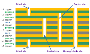
PCB interconnects come in three primary forms:
- Through vias: Penetrate all layers of the board
- Blind vias: Connect an outer layer to one or more inner layers
- Buried vias: Connect only inner layers without reaching either surface
Blind vias offer distinct advantages over through vias by conserving board space (no unused through-hole barrel occupying multiple layers) and enabling higher routing density. Compared to buried vias, blind vias provide easier testing access and simpler registration during manufacturing.
2. Manufacturing Processes for Blind Via PCBs
2.1 Laser Drilling Methods
Modern blind via formation primarily employs laser drilling techniques:
- CO₂ lasers (wavelength 9.4-10.6 μm): Effective for organic materials but cannot ablate copper
- UV lasers (wavelength 355 nm): Can drill through copper and dielectric, offering higher precision
- Excimer lasers: Provide extremely fine resolution but with lower throughput
The laser drilling process typically follows these steps:
- Surface copper patterning to define via locations
- Laser ablation through copper opening and dielectric material
- Desmearing to remove residual debris
- Electroless copper deposition to make holes conductive
- Electrolytic copper plating to build up thickness
2.2 Sequential Lamination Approach
Many blind via PCBs require multiple lamination cycles:
- Fabricate core substrate with conventional through holes
- Laminate additional dielectric and copper foil layers
- Laser drill blind vias through new layers
- Plate and pattern the new vias and circuitry
- Repeat process for additional blind via layers
This sequential build-up method enables complex multilayer structures with different blind via configurations at various levels of the board stack-up.
2.3 Photo-Defined Via Formation
Alternative processes use photosensitive dielectric materials:
- Apply photoimageable dielectric (PID) coating
- Expose through photomask to define via patterns
- Develop to remove unexposed material, creating via holes
- Metallize formed vias through plating processes
Photo-defined methods offer excellent dimensional control but may have limitations in material selection and thermal performance.
3. Design Considerations for Blind Via PCBs
3.1 Stack-up Planning
Effective blind via implementation requires careful layer stack-up design:
- Determine which layers require interconnection
- Plan via depths according to dielectric thicknesses
- Consider aspect ratio limitations for reliable plating
- Account for cumulative tolerances in multilayer designs
3.2 Signal Integrity Factors
Blind vias impact high-speed signal performance:
- Shorter via stubs reduce signal reflections
- Proper via transition design maintains impedance continuity
- Via-to-via spacing affects crosstalk in dense layouts
- Return current paths must be properly maintained
3.3 Thermal Management
Design considerations for heat dissipation:
- Blind vias can serve as thermal conduits to inner layers
- Via fill materials affect heat transfer characteristics
- Differential thermal expansion between materials
- Current carrying capacity and heat generation
3.4 Reliability and Testing
Designing for manufacturability and reliability:
- Via-in-pad designs require special processing
- Thermal cycling performance requirements
- Inspection and testing access considerations
- Failure modes and stress concentration points
4. Advantages and Limitations of Blind Via Technology
4.1 Key Benefits
Blind via PCBs offer numerous advantages:
Space Utilization:
- Enables higher component density
- Reduces board size requirements
- Allows for finer pitch components
Electrical Performance:
- Shorter interconnects improve signal speed
- Reduced via stub lengths enhance signal integrity
- Better impedance control in high-speed designs
Design Flexibility:
- Enables complex multilayer architectures
- Supports advanced packaging technologies
- Facilitates mixed-technology integration
4.2 Technical Challenges
Implementation challenges include:
Manufacturing Complexity:
- Additional process steps increase cost
- Tight registration requirements
- Specialized equipment needed
Reliability Concerns:
- Plating quality in high aspect ratio vias
- Thermal stress at via interfaces
- Long-term mechanical stability
Cost Factors:
- Higher raw material costs
- Increased processing time
- Lower yields compared to conventional PCBs
5. Applications of Blind Via PCBs
5.1 Consumer Electronics
Blind via technology enables feature-packed portable devices:
- Smartphones and tablets
- Wearable devices
- Digital cameras
- Gaming consoles
5.2 Computing Systems
High-performance computing applications:
- Server motherboards
- High-end graphics cards
- Solid-state drives
- Network processing units
5.3 Automotive Electronics
Advanced automotive systems:
- Engine control units
- Advanced driver assistance systems (ADAS)
- Infotainment systems
- Vehicle networking modules
5.4 Medical Devices
Medical electronics benefiting from blind vias:
- Implantable devices
- Diagnostic equipment
- Medical imaging systems
- Portable monitoring devices
5.5 Aerospace and Defense
Mission-critical applications:
- Avionics systems
- Satellite electronics
- Radar and communication systems
- Military-grade computing
6. Future Trends in Blind Via Technology
6.1 Advanced Materials Development
Emerging materials enhance blind via performance:
- Low-loss dielectrics for high-frequency applications
- High-thermal-conductivity substrates
- Flexible and stretchable interconnect materials
- Embedded passive materials
6.2 Manufacturing Innovations
Process improvements driving the technology forward:
- Higher precision laser systems
- Additive manufacturing approaches
- Automated optical inspection advancements
- Improved plating chemistry and processes
6.3 3D Packaging Integration
Blind vias enabling advanced packaging:
- Chip-last and chip-first embedded die
- Fan-out wafer-level packaging (FOWLP)
- Silicon interposers with through-silicon vias (TSVs)
- Heterogeneous integration approaches
6.4 Industry 4.0 and Smart Manufacturing
Digital transformation impacts:
- AI-assisted design tools
- Predictive process control
- Digital twin implementations
- Automated quality assurance systems
7. Conclusion
Blind via PCB technology has become indispensable for modern electronic packaging, offering unparalleled interconnect density and electrical performance. As electronic devices continue advancing toward higher speeds, smaller form factors, and greater functionality, blind vias will play an increasingly critical role in PCB design and manufacturing.
The technology presents both opportunities and challenges—while enabling groundbreaking products across industries, it demands specialized expertise in design, materials science, and manufacturing processes. Engineers must carefully evaluate when and how to implement blind vias, balancing performance requirements against cost and reliability considerations.
Future developments in materials, equipment, and design methodologies promise to further enhance blind via capabilities, ensuring their continued relevance in next-generation electronics. As the industry moves toward more sophisticated 3D packaging and heterogeneous integration schemes, blind via technology will likely evolve in tandem, maintaining its position as a cornerstone of advanced PCB fabrication.


