Build pcb
Step-by-Step Guide to Designing Your First PCB
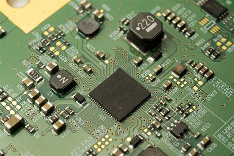
Designing your first printed circuit board (PCB) can be an exciting yet challenging endeavor. It requires a blend of creativity, technical knowledge, and attention to detail. To begin with, understanding the fundamental purpose of a PCB is crucial. A PCB serves as the backbone of electronic devices, providing mechanical support and electrical connections for various components. As you embark on this journey, it is essential to follow a structured approach to ensure a successful design.
The initial step in designing a PCB involves defining the requirements and specifications of your project.
This includes determining the size, shape, and functionality of the board. It is important to consider the components you plan to use, as well as their placement and orientation. By clearly outlining these parameters, you set a solid foundation for the subsequent stages of the design process.
Once the requirements are established, the next phase involves creating a schematic diagram.
This diagram serves as a blueprint for your PCB, illustrating the electrical connections between components. Utilizing schematic capture software, you can efficiently draft and organize your circuit design. It is advisable to double-check the connections and ensure that all components are correctly represented. This step is critical, as any errors in the schematic can lead to issues in the final PCB.
Following the schematic design, the next step is to transition to the layout phase.
This involves translating the schematic into a physical representation of the PCB. During this stage, you will arrange the components on the board and route the electrical traces that connect them. It is essential to consider factors such as signal integrity, thermal management, and manufacturability. By strategically placing components and optimizing trace routing, you can enhance the performance and reliability of your PCB.
As you progress through the layout process, it is important to pay attention to design rules and constraints.
These guidelines ensure that your PCB meets industry standards and can be manufactured without issues. Design rule checks (DRC) can be performed using PCB design software to identify any violations or potential problems. By addressing these issues early on, you can avoid costly mistakes and delays in production.
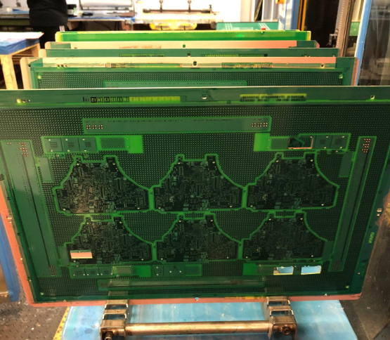
Once the layout is complete, the next step involves generating the necessary files for manufacturing.
These files, commonly known as Gerber files, contain all the information required to fabricate your PCB. It is crucial to review these files thoroughly to ensure accuracy and completeness. Additionally, you may need to provide a bill of materials (BOM) that lists all the components used in your design.
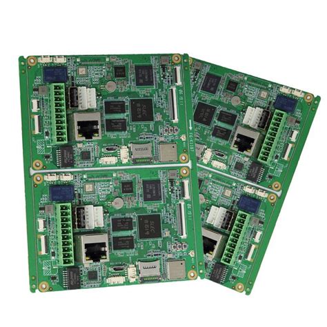
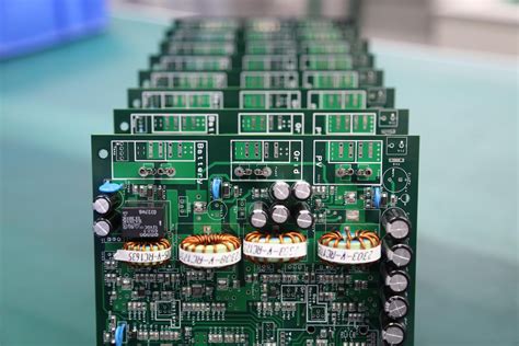
With the files prepared, you can proceed to the manufacturing stage.
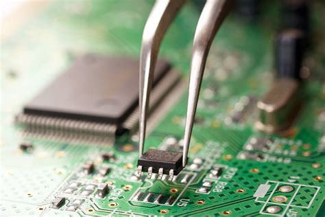
Selecting a reputable PCB manufacturer is vital to ensure high-quality production. It is advisable to communicate with the manufacturer to clarify any specific requirements or concerns. Once the PCB is fabricated, it undergoes assembly, where components are soldered onto the board. This process requires precision and attention to detail to ensure proper functionality.
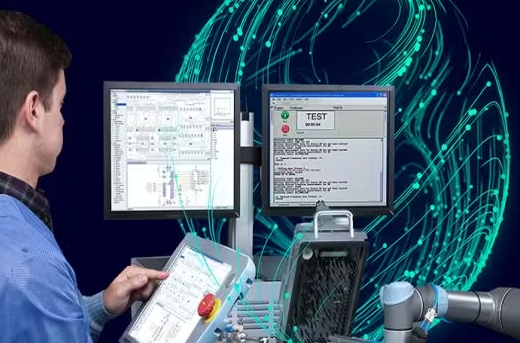
Finally, after assembly, it is essential to conduct thorough testing and validation of your PCB.
This involves checking for electrical continuity, verifying component functionality, and performing any necessary troubleshooting. By rigorously testing your design, you can identify and rectify any issues before deploying the PCB in its intended application.
In conclusion, designing your first PCB is a rewarding experience that requires careful planning and execution. By following a systematic approach, from defining requirements to testing the final product, you can create a reliable and efficient PCB that meets your project’s needs.
Top Software Tools for PCB Design and Simulation
Printed Circuit Boards (PCBs) are the backbone of modern electronic devices, serving as the foundation upon which electronic components are mounted and interconnected. The design and simulation of PCBs are critical steps in the development of any electronic product, ensuring functionality, reliability, and manufacturability. As technology advances, the complexity of PCBs increases, necessitating the use of sophisticated software tools to aid in their design and simulation. In this context, several top-tier software tools have emerged, each offering unique features and capabilities that cater to different aspects of PCB design and simulation.
To begin with, Altium Designer is widely regarded as one of the most comprehensive PCB design tools available.
It offers a unified design environment that integrates schematic capture, PCB layout, and design rule checking, among other features. Altium Designer is particularly favored for its user-friendly interface and powerful simulation capabilities, which allow designers to visualize and test their designs before proceeding to manufacturing. Furthermore, its extensive library of components and real-time collaboration features make it an ideal choice for teams working on complex projects.
Transitioning to another prominent tool, Eagle, developed by Autodesk, is known for its flexibility and affordability.
Eagle provides a robust platform for schematic capture and PCB layout, with a strong emphasis on customization. Its modular design allows users to tailor the software to their specific needs, making it suitable for both hobbyists and professional engineers. Additionally, Eagle’s integration with Autodesk’s Fusion 360 enables seamless transition from electronic design to mechanical design, facilitating a holistic approach to product development.
In contrast, KiCad stands out as a powerful open-source alternative that has gained significant traction in the PCB design community.
KiCad offers a suite of tools for schematic capture, PCB layout, and 3D visualization, all without the cost associated with proprietary software. Its open-source nature encourages community-driven development and continuous improvement, resulting in a tool that is both versatile and reliable. KiCad’s ability to handle complex designs and its support for a wide range of file formats make it a compelling choice for designers seeking a cost-effective solution.
Moving on to another noteworthy tool, OrCAD, developed by Cadence, is renowned for its advanced simulation capabilities.
OrCAD provides a comprehensive suite of tools for PCB design, including powerful simulation features that allow for detailed analysis of signal integrity, power integrity, and thermal performance. This makes OrCAD particularly suitable for high-performance applications where precision and reliability are paramount. Moreover, its integration with other Cadence tools enables a seamless workflow from design to manufacturing.
Finally, DipTrace offers an intuitive interface and a range of features that cater to both beginners and experienced designers.
DipTrace’s strength lies in its ease of use, with a focus on simplifying the design process without sacrificing functionality. It provides a comprehensive set of tools for schematic capture, PCB layout, and 3D modeling, along with a rich library of components. DipTrace’s affordability and user-friendly approach make it an attractive option for small businesses and individual designers.
In conclusion, the selection of a PCB design and simulation tool depends on various factors, including the complexity of the project, budget constraints, and specific design requirements. Each of the aforementioned tools offers distinct advantages, and understanding these can help designers make informed decisions that align with their project goals. As technology continues to evolve, these tools will undoubtedly adapt and improve, further enhancing the capabilities of PCB designers worldwide.

Common Mistakes to Avoid When Building a PCB
Building a printed circuit board (PCB) is a complex process that requires precision and attention to detail. However, even experienced engineers can fall prey to common mistakes that can compromise the functionality and reliability of the final product. Understanding these pitfalls is crucial for anyone involved in PCB design and manufacturing. One of the most frequent errors is inadequate planning during the design phase. It is essential to have a clear understanding of the circuit requirements and constraints before beginning the layout. Failing to do so can lead to design flaws that are difficult to rectify later in the process. Therefore, thorough planning and schematic verification are indispensable steps that should not be overlooked.
Another common mistake is neglecting to consider the thermal management of the PCB.
Components generate heat, and if this heat is not properly dissipated, it can lead to overheating and eventual failure of the board. To avoid this, designers should incorporate adequate heat sinks, thermal vias, and consider the placement of components to ensure efficient heat distribution. Additionally, using materials with appropriate thermal conductivity can significantly enhance the board’s performance.
Transitioning to the topic of component placement, it is crucial to ensure that components are placed logically and efficiently.
Poor component placement can lead to increased signal interference and longer trace lengths, which can degrade the performance of the PCB. Designers should aim for a layout that minimizes trace lengths and avoids crossing signals whenever possible. This not only improves the electrical performance but also simplifies the manufacturing process.
Furthermore, overlooking the importance of trace width and spacing is another common oversight.
Traces that are too narrow may not be able to handle the required current, leading to potential failures. On the other hand, traces that are too wide can take up unnecessary space and complicate the layout. It is important to calculate the appropriate trace width based on the current-carrying requirements and ensure that there is adequate spacing between traces to prevent short circuits and crosstalk.
In addition to these design considerations, it is also vital to pay attention to the selection of materials and components.
Using substandard or inappropriate materials can lead to issues such as delamination, warping, or poor electrical performance. Therefore, selecting high-quality materials that meet the specific requirements of the application is essential. Similarly, choosing the right components and ensuring their compatibility with the overall design can prevent many potential problems.
Moreover, failing to conduct thorough testing and validation of the PCB design can result in undetected errors that manifest during production or operation.
It is important to perform simulations and prototype testing to identify and rectify any issues before mass production. This step can save significant time and resources by preventing costly rework or redesigns.
Finally, communication and collaboration among team members are often underestimated aspects of PCB design.
Miscommunication can lead to misunderstandings and errors in the design process. Therefore, maintaining clear and open lines of communication among all stakeholders, including designers, engineers, and manufacturers, is crucial for the successful completion of a PCB project.
In conclusion, while building a PCB involves numerous challenges, being aware of and avoiding these common mistakes can greatly enhance the quality and reliability of the final product. By focusing on careful planning, efficient design practices, and thorough testing, engineers can ensure that their PCBs meet the desired specifications and perform optimally in their intended applications.
Innovative Techniques for Prototyping PCBs at Home
Prototyping printed circuit boards (PCBs) at home has become increasingly accessible due to advancements in technology and the availability of innovative techniques. As electronics enthusiasts and engineers seek to bring their designs to life without the need for industrial facilities, understanding these methods is crucial. The process of building PCBs at home not only fosters creativity but also accelerates the development cycle, allowing for rapid testing and iteration.
One of the most popular techniques for home PCB prototyping is the use of computer-aided design (CAD) software.
These programs enable designers to create detailed schematics and layouts, which can then be translated into physical boards. With a plethora of free and paid options available, such as KiCad and Eagle, users can select a tool that best fits their needs and expertise. Once the design is complete, the next step involves transferring it onto a physical medium.
A widely adopted method for transferring PCB designs is the toner transfer process.
This technique involves printing the PCB layout onto a special transfer paper using a laser printer. The printed design is then ironed onto a copper-clad board, where the heat causes the toner to adhere to the copper surface. After cooling, the board is submerged in an etching solution, typically ferric chloride, which removes the exposed copper, leaving behind the desired circuit pattern. This method is favored for its simplicity and cost-effectiveness, although it requires careful handling of chemicals and precise execution to achieve optimal results.
In addition to toner transfer, another innovative approach is the use of direct inkjet printing.
This technique leverages modified inkjet printers to deposit conductive ink directly onto a substrate, forming the circuit traces. While this method requires specialized equipment and materials, it offers the advantage of eliminating the need for etching, thus reducing chemical waste and environmental impact. Moreover, direct inkjet printing allows for greater flexibility in design changes, as modifications can be made quickly without the need for new masks or templates.
For those seeking a more advanced solution, CNC milling machines present an attractive option.
These machines can precisely carve out circuit patterns from copper-clad boards, offering high accuracy and repeatability. Although the initial investment in a CNC machine may be significant, the long-term benefits include the ability to produce complex multilayer boards and the elimination of chemical processes. Furthermore, CNC milling is well-suited for small production runs, making it ideal for hobbyists and small-scale developers.
As technology continues to evolve, the integration of 3D printing with PCB prototyping is gaining traction.
By using conductive filaments, 3D printers can create three-dimensional circuit structures, opening up new possibilities for innovative designs and applications. This approach not only streamlines the prototyping process but also enables the creation of unique form factors that were previously unattainable with traditional methods.
In conclusion, the landscape of home PCB prototyping is rich with innovative techniques that cater to a wide range of needs and expertise levels. From traditional methods like toner transfer to cutting-edge technologies such as direct inkjet printing and 3D printing, enthusiasts and engineers have a plethora of options to explore. As these techniques continue to develop, they promise to further democratize the field of electronics design, empowering individuals to transform their ideas into tangible realities with greater ease and efficiency.