Can Vias Be Placed on Pads in PCB Design?
Introduction
Printed Circuit Board (PCB) design involves numerous critical decisions that affect signal integrity, manufacturability, and reliability. One common debate among PCB designers is whether vias should be placed directly on pads (also known as via-in-pad). Traditionally, vias were kept away from pads to avoid soldering issues, but modern manufacturing techniques have made via-in-pad a viable option in many cases.
This article explores the advantages, disadvantages, and best practices of placing vias on pads in PCB design. We will examine the impact on signal integrity, thermal management, manufacturability, and assembly processes.
What Are Vias and Pads in PCB Design?
Before discussing via-in-pad, it’s essential to understand the basic definitions:
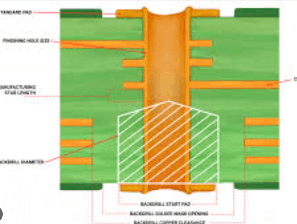
- Vias: Conductive holes that connect different layers of a PCB, allowing electrical signals or power to pass between layers.
- Pads: The exposed metal areas on a PCB where components are soldered.
Traditionally, vias were placed near pads but not directly on them to prevent solder wicking (where solder flows into the via instead of forming a proper joint). However, with advancements in PCB fabrication, via-in-pad has become more common, especially in high-density designs.
Advantages of Via-in-Pad
1. Improved Signal Integrity in High-Speed Designs
In high-frequency and high-speed PCB designs, minimizing inductance and ensuring a low-impedance return path are crucial. Placing vias directly on pads reduces the stub length of the signal path, which can help:
- Reduce parasitic inductance.
- Improve signal integrity by minimizing reflections.
- Enhance high-speed signal performance (e.g., in RF and microwave circuits).
2. Space Savings in High-Density Designs
Modern PCBs, especially those used in smartphones, wearables, and IoT devices, require extremely compact layouts. Via-in-pad allows designers to:
- Reduce the PCB footprint by eliminating extra space for vias.
- Enable finer pitch component placement (e.g., for BGA and QFN packages).
3. Better Thermal Management
For power electronics and high-current applications, vias on pads help dissipate heat more efficiently. This is particularly useful for:
- Power components (e.g., MOSFETs, voltage regulators).
- Thermal vias under ICs to transfer heat to ground planes or heatsinks.
4. Enhanced Electrical Performance
Via-in-pad reduces loop inductance, which is critical for:
- Decoupling capacitors (placing vias directly on capacitor pads minimizes inductance).
- Power distribution networks (PDNs) to ensure stable voltage delivery.
Disadvantages and Challenges of Via-in-Pad
1. Solder Wicking and Assembly Issues
The primary concern with via-in-pad is solder flowing into the via during reflow soldering, leading to:
- Weak solder joints.
- Insufficient solder for proper component attachment.
- Potential open connections or reliability issues.
2. Increased Manufacturing Cost
Via-in-pad requires additional PCB fabrication steps, such as:
- Via filling (with conductive or non-conductive epoxy).
- Planarization (to ensure a flat surface for soldering).
- More precise drilling and plating processes.
These extra steps can increase production costs, making via-in-pad less economical for low-cost PCBs.
3. Potential for Void Formation
If vias are not properly filled, trapped air or gases can expand during soldering, leading to:
- Voids in solder joints.
- Reduced mechanical strength.
- Long-term reliability concerns.
4. Difficulty in Rework and Repair
Components soldered over filled vias can be harder to rework because:
- The filled via may retain heat differently, complicating desoldering.
- Removing components without damaging the PCB is more challenging.
Best Practices for Via-in-Pad Implementation
To successfully use via-in-pad, designers should follow these guidelines:
1. Use Filled and Capped Vias
- Conductive epoxy filling: Ensures electrical continuity and prevents solder wicking.
- Non-conductive filling: Used when electrical isolation is needed.
- Copper capping: Provides a flat surface for soldering.
2. Apply Proper Via Sizing
- Smaller vias (e.g., 0.1–0.2mm) are easier to fill and cap.
- Avoid excessively large vias, which increase the risk of solder wicking.
3. Consult PCB Fabrication Guidelines
- Different manufacturers have varying capabilities for via filling (e.g., laser-drilled microvias vs. mechanically drilled vias).
- Ensure the chosen PCB supplier supports via-in-pad technology.
4. Optimize for Assembly Processes
- Use solder mask plugging if via filling is not an option.
- Adjust reflow profiles to account for thermal differences caused by vias.
5. Simulation and Testing
- Perform signal integrity simulations (e.g., in HyperLynx or Ansys HFSS) to assess via-in-pad effects.
- Test thermal performance to ensure proper heat dissipation.
When to Avoid Via-in-Pad
Despite its advantages, via-in-pad is not always the best choice. Avoid it in:
- Low-cost PCBs where additional fabrication expenses are prohibitive.
- Hand-soldered or prototype boards where reworkability is critical.
- Designs with large through-hole vias that cannot be reliably filled.
Conclusion
The decision to place vias on pads depends on the specific PCB design requirements. While via-in-pad offers significant benefits in high-speed, high-density, and thermal-critical applications, it also introduces manufacturing complexities and potential assembly challenges.
Designers must weigh the trade-offs and collaborate with PCB manufacturers to ensure successful implementation. With proper via filling, capping, and adherence to best practices, via-in-pad can be a powerful tool in modern PCB design.
By understanding the advantages, limitations, and techniques for mitigating risks, engineers can leverage via-in-pad technology to enhance performance while maintaining reliability.


