Case Study on Methods to Prevent Defects in PCB Manufacturing
1.Introduction
In the modern electronic product world, PCB (printed circuit board) is an important part of electronic products. It is hard to imagine that there is no PCB in an electronic device, so the quality of PCB will have a great impact on whether the electronic product can work normally and reliably for a long time. Improving the quality of PCB is an important topic that electronic product manufacturers should pay enough attention to.
PCB Circuit Board
If excessive solder paste is applied to the pad during the assembly process of PCB, or insufficient solder paste is added, or even no solder paste is placed at all, then after the subsequent reflow soldering, once the solder joint is formed, it will cause defects in the electronic connection between the components and the circuit board. In fact, most defects can be found with the help of the application of solder paste.
Currently, many circuit board manufacturers have adopted some built-in circuit tests (in-circujt test, abbreviated as lCT) or X-ray technology to detect the quality of solder joints. They will help eliminate defects caused by printing process operations, but these methods cannot monitor the printing process operations themselves. A printed circuit board with an error may be subject to subsequent process steps, each of which will increase production costs to varying degrees, causing such a defective circuit board to eventually reach the placement stage of production. Finally, the manufacturer needs to discard the defective circuit board or accept costly and time-consuming rework work. At this time, there may be no very clear answer to explain the root cause of the defect.
Poor solder paste printing process implementation can cause connection problems in electronic circuits. In order to effectively solve this problem, many screen printing equipment manufacturers have adopted online machine vision inspection technology, which is briefly introduced below.

2.Online comprehensive visual inspection
In order to help circuit board manufacturers detect defects in the early stages of production process implementation, more and more screen printing equipment manufacturers are integrating online machine vision technology in their screen printing equipment. Built-in vision systems can achieve three main goals:
First, they can detect existing defects directly after the printing operation is implemented, allowing operators to deal with related problems in a timely manner before major manufacturing costs are added to the circuit board. This step is generally included when the board is removed from the printing device, after it is cleaned in the cleaning agent, and when it is returned to the production line after rework.
Secondly, because the relevant defects are found at this stage, defective boards can be prevented from being sent to the back end of the production line. Thus, rework or waste in some cases is prevented.
Finally, and perhaps most importantly: timely feedback can be given to the operator to make it clear whether the printing process in operation is operating well, which can effectively prevent the occurrence of defects.
In order to provide effective control during the process operation at this level, the configuration of the online vision system can detect the condition of the pads on the PCB after the solder paste is applied, and whether the corresponding printing template gap is blocked or tailing. In most cases, the inspection of fine-pitch components is to optimize the inspection time and focus on the areas most prone to problems. For this reason, when the possible problems are eliminated, the time spent on inspection is still worthwhile.

3.Camera positioning and detection
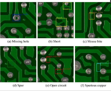
In general conventional online visual inspection applications, the camera is placed above the circuit board to obtain images of the printing position and can send the relevant images to the processing system of the visual inspection equipment. There, the image analysis software will compare the acquired image with the reference image stored in the same position in the device memory. In this way, the system can confirm whether the applied solder paste is too much or too little. The system can also reveal whether the solder paste position on the pad is aligned. It can find out whether there is excess solder paste between two pads to form a bridge-like connection phenomenon? This problem is also commonly known as the “bridging” phenomenon by many printed circuit board manufacturers.
The work of detecting the gap of the printing template is in the same form. When excess solder paste is accumulated on the surface of the printing template, the visual system can be used to detect whether the gap is blocked by solder paste or whether tailing occurs. After the defect is found, the equipment can automatically request a series of cleaning operations for the screen below, or alert the operator that there is a problem that needs to be repaired. The detection of the printing template can also provide users with very useful data on printing quality and consistency.
A key feature of the most advanced online vision systems is the ability to inspect highly reflective PCB and pad surfaces, as well as in non-uniform light environments or under conditions where there are differences in the structure of dried solder paste. For example, HASL boards generally exhibit uneven flatness, variable surface contours and reflective properties. To obtain the highest quality images, appropriate lighting also plays a very important role. The light must be able to “target” the board’s fiducials and pads, turning other subtle features into clearly recognizable shapes. This allows the next step to use vision software algorithms to fully realize their potential.
In some specific cases, vision systems can be used to detect the height or volume of solder paste on pads, which may sometimes only be done by offline inspection systems. Using this procedure means forming a corresponding accumulation in a given printing template to confirm whether the volume of solder paste is missing on the same pad.

4.Solder paste detection
It can be divided into two categories: detection of solder paste on PCB and detection of solder paste on printing template:
a. PCB inspection
Mainly inspect the printing area, printing offset and bridging phenomenon. The inspection of the printing area refers to the solder paste area on each pad. Excessive solder paste may cause bridging phenomenon, and too little solder paste may also cause the solder joint to be loose. The inspection of printing offset is to check whether the amount of solder paste on the pad is different from the specified position. The inspection of bridging phenomenon is to check whether the solder paste applied between two adjacent pads exceeds the specified amount. These excess solder pastes may cause electrical short circuits.
b. Inspection of printing templates
The inspection of printing templates is mainly for the detection of blocking and tailing phenomena. The inspection of blocking refers to the inspection of whether solder paste is accumulated in the holes on the printing template. If the holes are blocked, the solder paste applied to the next printing point may appear too little. The inspection of tailing refers to whether there is excessive solder paste accumulated on the surface of the printing template. These excess solder pastes may be applied to the position on the circuit board that should not be conductive, thereby causing electrical connection problems.
5.Conclusion
Online machine vision systems can benefit PCB manufacturers in different ways. In addition to ensuring the high integrity of solder joints, it can prevent manufacturers from wasting money due to board defects and the resulting rework. Perhaps most importantly, it can provide continuous process feedback, which can not only help manufacturers optimize the screen printing process, but also add more confidence during the process operation.


