Castellated PCBs: Design, Applications, and Manufacturing Considerations
Introduction
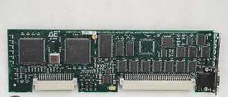
Printed Circuit Boards (PCBs) are essential components in modern electronics, providing the foundation for electrical connections between components. Among the various types of PCBs, castellated PCBs (also known as castellated holes or castellations) play a crucial role in modular electronics, system-on-module (SoM) designs, and board-to-board connections.
Castellated PCBs feature plated half-holes along the edges of the board, allowing them to be surface-mounted onto another PCB. This design enables easy integration, modularity, and compact assembly, making them popular in applications such as Wi-Fi modules, Bluetooth modules, and embedded systems.
This article explores the design principles, manufacturing process, advantages, and applications of castellated PCBs, providing a comprehensive guide for engineers and designers.
1. What Are Castellated PCBs?
Castellated PCBs are characterized by semi-plated through-holes (PTHs) machined along the edges of the board, creating a series of “castles” or notches. These castellations allow the PCB to be soldered directly onto another board, similar to a surface-mount device (SMD).
Key Features:
- Half-holes along the edges (partially drilled and plated).
- Used for board-to-board soldering (eliminating the need for connectors).
- Improves modularity (easier replacement and upgrades).
- Space-efficient compared to traditional interconnects.
2. Design Considerations for Castellated PCBs
Designing castellated PCBs requires careful attention to hole placement, plating, and mechanical stability. Below are critical design factors:
2.1. Castellated Hole Specifications
- Diameter & Spacing:
- Standard hole diameters range from 0.5mm to 1.5mm.
- Spacing between holes should allow sufficient solder flow without bridging.
- Plating Thickness:
- Typically 20-30µm copper plating ensures reliable conductivity.
- Edge Clearance:
- Maintain at least 0.2mm clearance from the board edge to prevent cracking.
2.2. PCB Material & Thickness
- FR-4 is the most common substrate, but high-frequency applications may use Rogers or polyimide.
- Recommended thickness: 0.8mm to 1.6mm (thicker boards provide better mechanical stability).
2.3. Solder Mask & Silkscreen
- Solder mask should not cover castellations to ensure proper soldering.
- Silkscreen markings help with alignment during assembly.
2.4. Thermal & Mechanical Stress Management
- Thermal relief pads prevent excessive heat dissipation during soldering.
- Reinforced edges (using additional copper or stiffeners) prevent breakage.
3. Manufacturing Process of Castellated PCBs
Producing castellated PCBs involves precision drilling, plating, and routing. Below is a step-by-step overview:
3.1. Drilling Full Through-Holes
- Standard mechanical or laser drilling creates full through-holes along the intended edge.
3.2. Plating the Holes
- Electroless copper deposition followed by electroplating ensures conductivity.
3.3. Routing the Board Edge
- A CNC router cuts the board in half, splitting the plated holes into semi-circles.
- Deburring smoothens the edges to prevent copper peeling.
3.4. Solder Mask Application
- Liquid photoimageable solder mask (LPI) is applied, avoiding the castellations.
3.5. Surface Finish (Optional)
- HASL (Hot Air Solder Leveling), ENIG (Electroless Nickel Immersion Gold), or OSP (Organic Solderability Preservative) improves solderability.
4. Advantages of Castellated PCBs
Castellated PCBs offer several benefits over traditional interconnects:
4.1. Space Efficiency
- Eliminates the need for bulky connectors, saving up to 30% board space.
4.2. Improved Signal Integrity
- Shorter signal paths reduce inductance and crosstalk in high-speed designs.
4.3. Modularity & Ease of Replacement
- Modules can be easily swapped without desoldering entire boards.
4.4. Cost-Effective Assembly
- Reduces connector costs and simplifies inventory management.
5. Common Applications of Castellated PCBs
Castellated PCBs are widely used in modular and compact electronics:
5.1. Wireless Communication Modules
- Wi-Fi, Bluetooth, and LoRa modules (e.g., ESP32, nRF52).
5.2. Embedded Systems
- Raspberry Pi Compute Module, System-on-Module (SoM) designs.
5.3. IoT & Wearable Devices
- Small form-factor sensors and edge computing devices.
5.4. Power Modules
- DC-DC converters and voltage regulators.
6. Challenges & Solutions
Despite their advantages, castellated PCBs present some challenges:
| Challenge | Solution |
|---|---|
| Solder bridging | Use solder paste stencils with proper aperture design. |
| Mechanical fragility | Reinforce edges with additional copper or epoxy. |
| Misalignment during assembly | Include fiducial marks for precise placement. |
| Thermal stress cracks | Use thermal relief connections and avoid rapid cooling. |
7. Future Trends in Castellated PCB Technology
- Laser-drilled micro-castellations for ultra-compact designs.
- Advanced materials (flex PCBs with castellations for wearables).
- Automated optical inspection (AOI) for defect detection.
Conclusion
Castellated PCBs provide an efficient, cost-effective solution for modular electronics, compact designs, and reliable board-to-board connections. By following proper design guidelines and manufacturing techniques, engineers can leverage castellations to enhance product performance and scalability.
As technology advances, castellated PCBs will continue to play a vital role in IoT, wireless communications, and embedded systems, driving innovation in electronics miniaturization and modular design.


