additive manufacturing pcb | additive pcb | additive pcb manufacturing | advanced assembly pcb | advanced circuit board | advanced circuits 4pcb | uncategories
Calculation of Parasitic Capacitance and Inductance in PCB Design
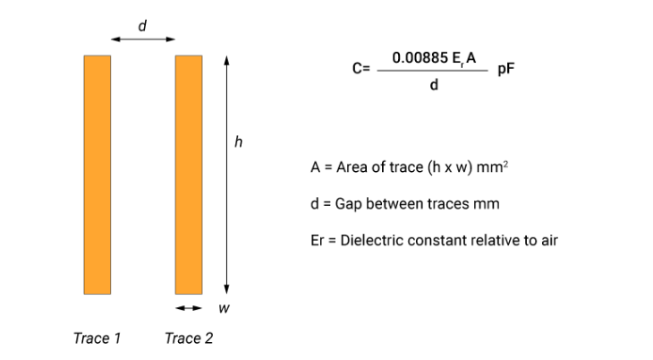
Abstract This paper provides a comprehensive analysis of parasitic capacitance and inductance in printed circuit board (PCB) designs. As modern electronics continue to operate at higher frequencies and with greater signal integrity requirements, understanding and calculating these parasitic elements becomes crucial for successful circuit implementation. The article presents theoretical foundations, calculation methods, and practical considerations…