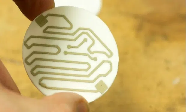
Ceramic pcb prototype
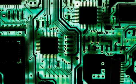
Advantages Of Using Ceramic PCB Prototypes In High-Frequency Applications
When it comes to high-frequency applications, the choice of materials can make or break the performance of your electronic devices.
One material that’s been gaining a lot of traction lately is ceramic, particularly in the form of ceramic PCB prototypes. You might be wondering why ceramic is becoming the go-to material for these applications. Well, let’s dive into the advantages and see why ceramic PCB prototypes are making waves in the tech world.
First off, one of the most compelling reasons to use ceramic PCBs in high-frequency applications is their excellent thermal conductivity.
Unlike traditional materials like FR4, ceramic can efficiently dissipate heat, which is crucial when dealing with high-frequency signals. This means your components are less likely to overheat, leading to a longer lifespan and more reliable performance. Imagine running a high-frequency circuit without worrying about it turning into a mini heater—sounds pretty good, right?
Another significant advantage is the low dielectric constant and low loss tangent of ceramic materials.
In simpler terms, this means that ceramic PCBs can handle high-frequency signals with minimal signal loss. This is particularly important in applications like RF (radio frequency) and microwave circuits, where maintaining signal integrity is paramount. With ceramic PCBs, you get a cleaner, more accurate signal, which can make all the difference in the world of high-frequency electronics.
Moreover, ceramic PCBs offer excellent mechanical stability.
They are less prone to warping and can withstand higher levels of mechanical stress compared to their traditional counterparts. This makes them ideal for applications that require a high degree of precision and reliability. For instance, in aerospace and military applications, where failure is not an option, ceramic PCBs provide that extra layer of assurance.
Transitioning to another key point, let’s talk about miniaturization.
As technology advances, there’s a growing demand for smaller, more compact devices. Ceramic PCBs are incredibly versatile in this regard. They allow for higher component density, meaning you can pack more functionality into a smaller space. This is a game-changer for industries like telecommunications and medical devices, where space is at a premium.
Additionally, ceramic PCBs are highly resistant to environmental factors such as moisture, chemicals, and extreme temperatures.
This makes them suitable for harsh environments where other materials might fail. For example, in automotive applications, where the PCB might be exposed to high temperatures and corrosive substances, ceramic PCBs can stand up to the challenge.
Now, you might be thinking, “This all sounds great, but what about the cost?” It’s true that ceramic PCBs can be more expensive than traditional materials.
However, when you consider the long-term benefits—such as improved performance, reliability, and longevity—the initial investment often pays off. Plus, as the technology becomes more widespread, the costs are likely to come down, making it a more accessible option for various applications.
In conclusion, the advantages of using ceramic PCB prototypes in high-frequency applications are numerous and compelling. From excellent thermal conductivity and low signal loss to mechanical stability and environmental resistance, ceramic PCBs offer a robust solution for modern electronic challenges. So, if you’re working on a high-frequency project and looking for a material that can keep up with your demands, ceramic PCBs might just be the answer you’ve been searching for.
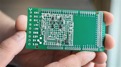
Step-By-Step Guide To Designing A Ceramic PCB Prototype
Designing a ceramic PCB prototype might sound like a daunting task, but with the right approach, it can be a rewarding experience. Whether you’re a seasoned engineer or a curious hobbyist, understanding the step-by-step process can make the journey smoother and more enjoyable. Let’s dive into the world of ceramic PCBs and explore how to create your very own prototype.
First things first, it’s essential to grasp why ceramic PCBs are so special.
Unlike traditional PCBs made from materials like FR4, ceramic PCBs offer superior thermal conductivity, excellent mechanical strength, and enhanced electrical insulation. These properties make them ideal for high-power applications, LED lighting, and even aerospace technology. With that in mind, let’s get started on designing your ceramic PCB prototype.
The initial step in the process is to define your requirements.
What is the purpose of your PCB? What components will you be using? Having a clear understanding of your project’s needs will guide you through the design process. Once you have a solid grasp of your requirements, it’s time to move on to the schematic design.
Creating a schematic is like drawing a blueprint for your PCB.
You’ll need to use a PCB design software, such as Altium Designer, Eagle, or KiCad, to lay out your circuit. This involves placing components like resistors, capacitors, and integrated circuits, and connecting them with virtual wires. It’s crucial to double-check your connections and ensure that your schematic is error-free before proceeding.
With your schematic in hand, the next step is to design the PCB layout.
This is where the magic happens, as you transform your 2D schematic into a 3D physical board. When working with ceramic PCBs, it’s important to consider factors like thermal management and mechanical stability. Ceramic materials can handle high temperatures, but you still need to ensure proper heat dissipation. Placing components strategically and using thermal vias can help manage heat effectively.
As you design the layout, pay attention to trace widths and spacing.
Ceramic PCBs can support fine traces, but it’s essential to follow the design rules provided by your manufacturer. Additionally, consider the placement of vias and pads, as these will affect the overall performance of your PCB. Once you’re satisfied with your layout, it’s time to generate the Gerber files.
Gerber files are the standard format used by PCB manufacturers to fabricate your design.
These files contain all the information needed to create your PCB, including the copper layers, solder mask, and silkscreen. Double-check your Gerber files to ensure they accurately represent your design. Any mistakes at this stage can lead to costly errors during manufacturing.
Now that you have your Gerber files, it’s time to choose a manufacturer.
Not all PCB manufacturers specialize in ceramic PCBs, so it’s essential to find one with experience in this area. Reach out to potential manufacturers, request quotes, and discuss your project requirements. Once you’ve selected a manufacturer, submit your Gerber files and place your order.
While waiting for your prototype to be fabricated, gather the necessary components for assembly
When your ceramic PCB arrives, inspect it carefully for any defects or issues. If everything looks good, proceed with assembling your components onto the board. This step requires precision and patience, as ceramic PCBs can be more fragile than their FR4 counterparts.
Finally, it’s time to test your prototype.
Power up your PCB and verify that it functions as expected. Troubleshoot any issues that arise and make necessary adjustments. This iterative process of testing and refining is crucial to achieving a successful ceramic PCB prototype.
In conclusion, designing a ceramic PCB prototype involves a series of well-defined steps, from defining your requirements to testing the final product. By following this guide and paying attention to the unique properties of ceramic materials, you can create a high-performance PCB that meets your project’s needs. Happy designing!
Comparing Ceramic PCB Prototypes To Traditional FR4 PCBs
When it comes to choosing the right material for your printed circuit board (PCB), the decision can be a bit overwhelming. With so many options available, it’s essential to understand the differences between them. One of the most intriguing comparisons is between ceramic PCB prototypes and traditional FR4 PCBs. Both have their unique advantages and disadvantages, and knowing these can help you make an informed decision for your next project.
First off, let’s talk about the basics.
FR4 is a widely used material in the PCB industry, known for its reliability and cost-effectiveness. It’s made from woven fiberglass cloth with an epoxy resin binder that is flame resistant. This material has been the go-to for many years due to its excellent electrical insulation properties and mechanical strength. However, as technology advances and the demand for more robust and high-performance PCBs increases, ceramic PCBs have started to gain traction.
Ceramic PCBs are made from ceramic materials like aluminum oxide, aluminum nitride, or beryllium oxide.
These materials offer several advantages over traditional FR4. For starters, ceramic PCBs have superior thermal conductivity. This means they can dissipate heat much more efficiently, making them ideal for high-power applications where managing heat is crucial. Think of LED lighting systems, power electronics, and RF applications. The ability to handle high temperatures without degrading makes ceramic PCBs a reliable choice for these demanding environments.
Moreover, ceramic PCBs exhibit excellent dimensional stability.
Unlike FR4, which can expand and contract with temperature changes, ceramic materials remain stable. This stability ensures that the components on the PCB stay in place, maintaining the integrity of the connections and reducing the risk of failure. This is particularly important in applications where precision is key, such as aerospace and medical devices.
On the flip side, there are some drawbacks to using ceramic PCBs.
One of the most significant is the cost. Ceramic materials are generally more expensive than FR4, which can be a limiting factor for budget-conscious projects. Additionally, the manufacturing process for ceramic PCBs is more complex, which can further drive up costs and lead times. This complexity also means that not all manufacturers have the capability to produce ceramic PCBs, potentially limiting your options.
Another point to consider is the mechanical strength.
While ceramic PCBs are excellent at handling heat, they are more brittle compared to FR4. This brittleness can make them more susceptible to cracking or breaking under mechanical stress. Therefore, if your application involves a lot of physical handling or is subject to vibrations, FR4 might be the more durable choice.
Despite these challenges, the benefits of ceramic PCBs often outweigh the drawbacks, especially for high-performance applications.
The decision ultimately comes down to the specific needs of your project. If thermal management and dimensional stability are critical, and you have the budget to accommodate the higher costs, ceramic PCBs could be the way to go. However, if you’re working on a more straightforward project with less demanding requirements, traditional FR4 PCBs might be perfectly adequate.
In conclusion, both ceramic PCB prototypes and traditional FR4 PCBs have their place in the world of electronics. By understanding the strengths and weaknesses of each, you can make a more informed decision that aligns with your project’s goals and constraints. Whether you opt for the high-performance capabilities of ceramic or the tried-and-true reliability of FR4, the key is to choose the material that best meets your specific needs.
Innovations In Ceramic PCB Prototyping Technology
Ceramic PCB prototyping has been making waves in the tech world, and for good reason. As technology continues to evolve at a breakneck pace, the demand for more efficient, durable, and high-performance materials has never been higher. Enter ceramic PCBs, which are quickly becoming the go-to choice for many engineers and designers. But what exactly makes ceramic PCBs so special, and how has recent innovation in prototyping technology made them even more appealing?
First off, let’s talk about the basics.
Traditional PCBs, or printed circuit boards, are typically made from materials like fiberglass or epoxy. While these materials have served us well for decades, they come with their own set of limitations. For instance, they can struggle with high temperatures and are not always the best at dissipating heat. This is where ceramic PCBs come into play. Made from materials like aluminum oxide, aluminum nitride, or beryllium oxide, ceramic PCBs offer superior thermal conductivity and can withstand much higher temperatures. This makes them ideal for applications in high-power electronics, aerospace, and even medical devices.
Now, you might be wondering, if ceramic PCBs are so great, why aren’t they everywhere?
The answer lies in the challenges associated with their production. Traditional methods of manufacturing ceramic PCBs can be time-consuming and expensive. However, recent innovations in prototyping technology are changing the game. One of the most exciting developments is the advent of additive manufacturing, or 3D printing, for ceramic PCBs. This technology allows for the rapid production of complex designs that would be difficult or impossible to achieve with traditional methods. Not only does this speed up the prototyping process, but it also reduces costs, making ceramic PCBs more accessible to a wider range of industries.
Moreover, advancements in laser processing technology have also played a significant role in the evolution of ceramic PCB prototyping.
Laser direct structuring (LDS) is a technique that uses a laser to create the circuit pattern directly on the ceramic substrate. This method is incredibly precise and allows for the creation of highly intricate designs. Additionally, it eliminates the need for masks and etching chemicals, making it a more environmentally friendly option.
Another noteworthy innovation is the development of hybrid ceramic PCBs.
These boards combine the best of both worlds by integrating ceramic materials with traditional PCB substrates. This hybrid approach offers enhanced performance while keeping costs relatively low. It’s a win-win situation that has caught the attention of many in the industry.
Furthermore, the use of advanced simulation software has revolutionized the design process for ceramic PCBs.
Engineers can now model and test their designs in a virtual environment before moving on to physical prototyping. This not only saves time but also allows for more iterations and optimizations, leading to better end products.
In conclusion, the world of ceramic PCB prototyping is undergoing a significant transformation, thanks to a slew of innovative technologies. From 3D printing and laser direct structuring to hybrid materials and advanced simulation software, these advancements are making ceramic PCBs more viable and attractive than ever before. As these technologies continue to evolve, we can expect to see even more exciting developments on the horizon. So, whether you’re an engineer, a designer, or just a tech enthusiast, it’s worth keeping an eye on this rapidly changing landscape. Who knows? The next big breakthrough in electronics might just be built on a ceramic PCB.