Ceramic pcb reflow profile
Understanding The Basics Of Ceramic PCB Reflow Profile
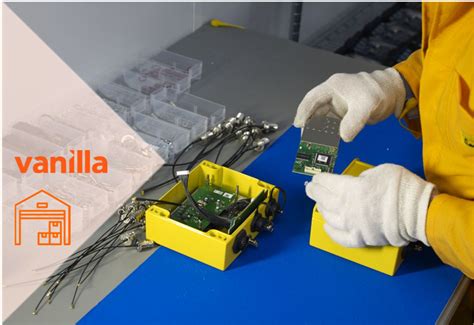
In the realm of electronics manufacturing, the reflow soldering process is a critical step that ensures the proper assembly of components onto printed circuit boards (PCBs). Among the various types of PCBs, ceramic PCBs are gaining prominence due to their superior thermal conductivity and mechanical stability. Understanding the basics of the ceramic PCB reflow profile is essential for achieving optimal soldering results and ensuring the reliability of electronic devices.
To begin with, the reflow profile is a temperature versus time graph that outlines the thermal cycle a PCB undergoes during the reflow soldering process.
This profile is crucial for controlling the heating and cooling rates, which in turn affect the quality of the solder joints. For ceramic PCBs, the reflow profile must be carefully tailored to accommodate their unique thermal properties. Unlike traditional FR-4 PCBs, ceramic substrates can withstand higher temperatures, which allows for a broader range of soldering conditions. However, this also necessitates precise control to prevent thermal shock and potential damage to the components.
The reflow profile typically consists of four main stages: preheat, soak, reflow, and cooling.
Each stage plays a vital role in ensuring the proper melting and solidification of the solder paste. During the preheat stage, the temperature is gradually increased to prevent thermal shock and to activate the flux in the solder paste.
This stage is particularly important for ceramic PCBs, as their high thermal conductivity can lead to rapid temperature changes if not carefully managed.
The soak stage follows, where the temperature is held steady to allow for the even distribution of heat across the board.
This helps in minimizing temperature gradients and ensuring uniform soldering.
Transitioning to the reflow stage, the temperature is raised to a peak level that exceeds the melting point of the solder alloy. For ceramic PCBs, this peak temperature can be higher than that used for traditional PCBs, thanks to their ability to withstand elevated temperatures.
However, it is crucial to avoid excessive temperatures that could damage sensitive components or cause warping of the ceramic substrate. The duration at peak temperature should be optimized to ensure complete melting of the solder without prolonged exposure that could lead to defects.
Finally, the cooling stage is where the temperature is gradually reduced to solidify the solder joints.
Controlled cooling is essential to prevent thermal stress and to ensure the mechanical integrity of the solder connections. For ceramic PCBs, the cooling rate must be carefully managed to avoid inducing cracks or other structural issues.
In conclusion, understanding the basics of the ceramic PCB reflow profile is fundamental for achieving high-quality soldering results.
The unique properties of ceramic substrates require a tailored approach to the reflow process, with careful attention to each stage of the thermal cycle. By optimizing the reflow profile, manufacturers can enhance the performance and reliability of electronic devices that utilize ceramic PCBs. As the demand for high-performance electronics continues to grow, mastering the intricacies of ceramic PCB reflow profiles will remain a critical aspect of advanced electronics manufacturing.
Optimizing Reflow Profiles For Ceramic PCBs
Optimizing reflow profiles for ceramic PCBs is a critical aspect of ensuring the reliability and performance of electronic assemblies. As the demand for high-performance electronic devices continues to grow, ceramic PCBs have emerged as a preferred choice due to their superior thermal conductivity, mechanical strength, and electrical insulation properties.
However, the unique characteristics of ceramic materials necessitate careful consideration during the reflow soldering process to achieve optimal results.
To begin with, understanding the thermal properties of ceramic substrates is essential.
Unlike traditional FR-4 boards, ceramic PCBs can withstand higher temperatures, which allows for a broader range of soldering profiles. However, this advantage also requires precise control over the reflow process to prevent potential issues such as thermal shock or warping. Therefore, selecting an appropriate reflow profile is crucial to maintaining the integrity of the ceramic material while ensuring proper solder joint formation.
The reflow profile typically consists of four main stages: preheat, soak, reflow, and cooling.
Each stage must be carefully calibrated to accommodate the specific thermal characteristics of ceramic PCBs. During the preheat stage, the temperature is gradually increased to prevent thermal shock and to ensure uniform heat distribution across the board. This gradual increase is particularly important for ceramic substrates, which can be more susceptible to cracking under rapid temperature changes.
Following the preheat stage, the soak phase allows for the stabilization of temperature across the PCB.
This stage is critical for activating the flux and ensuring that all components reach a uniform temperature before entering the reflow zone. For ceramic PCBs, maintaining a consistent soak temperature is vital to prevent differential expansion between the substrate and the components, which could lead to mechanical stress and potential failure.
The reflow stage is where the solder paste reaches its melting point, forming the necessary solder joints.
For ceramic PCBs, it is important to select a solder paste with a compatible melting temperature to avoid damaging the substrate. Additionally, the peak temperature and time above liquidus must be carefully controlled to ensure complete wetting of the solder joints without overheating the ceramic material. This balance is crucial to achieving strong, reliable connections that can withstand the operational demands of high-performance applications.
Finally, the cooling stage solidifies the solder joints and stabilizes the assembly.
A controlled cooling rate is essential to prevent thermal shock and to minimize the risk of introducing stress into the solder joints. For ceramic PCBs, a gradual cooling process helps maintain the structural integrity of both the substrate and the components, ensuring long-term reliability.
In conclusion, optimizing reflow profiles for ceramic PCBs requires a comprehensive understanding of the material’s thermal properties and careful calibration of each stage in the reflow process.
By selecting appropriate temperature profiles and controlling the heating and cooling rates, manufacturers can ensure the production of high-quality electronic assemblies that leverage the advantages of ceramic substrates. As technology continues to advance, the ability to fine-tune reflow profiles for ceramic PCBs will remain a critical factor in meeting the demands of increasingly sophisticated electronic devices.
Common Challenges In Ceramic PCB Reflow Profiling
Ceramic printed circuit boards (PCBs) are increasingly favored in high-performance applications due to their superior thermal conductivity, mechanical strength, and electrical insulation properties. However, the reflow profiling process for ceramic PCBs presents unique challenges that can impact the quality and reliability of the final product. Understanding these challenges is crucial for manufacturers aiming to optimize their production processes and ensure the highest standards of performance.
One of the primary challenges in ceramic PCB reflow profiling is the material’s inherent thermal characteristics.
Unlike traditional FR-4 boards, ceramic substrates such as alumina or aluminum nitride have significantly higher thermal conductivity. This property, while beneficial for heat dissipation during operation, complicates the reflow process. The rapid heat transfer can lead to uneven temperature distribution across the board, potentially causing soldering defects such as tombstoning or insufficient wetting. To mitigate this, manufacturers must carefully design their reflow profiles, ensuring a gradual and controlled temperature ramp-up to achieve uniform heating.
Moreover, the thermal expansion coefficient of ceramic materials differs from that of the solder and components used in assembly.
This discrepancy can result in mechanical stress during the heating and cooling phases of reflow, leading to issues such as component misalignment or even cracking of the ceramic substrate. To address this, it is essential to employ a reflow profile that minimizes thermal shock. This often involves extending the soak time to allow for thermal equilibrium and employing a controlled cooling rate to reduce stress.
Another challenge arises from the need for precise temperature control throughout the reflow process.
Ceramic PCBs often incorporate components that are sensitive to temperature variations, necessitating a high degree of accuracy in temperature profiling. Advanced reflow ovens equipped with multiple heating zones and sophisticated control systems are typically required to maintain the necessary precision. Additionally, regular calibration and maintenance of these ovens are crucial to ensure consistent performance and avoid deviations that could compromise the integrity of the solder joints.
Furthermore, the complexity of ceramic PCB designs can exacerbate reflow profiling challenges.
As these boards are often used in high-density applications, they may feature a variety of component sizes and types, each with different thermal mass and soldering requirements. This diversity necessitates a reflow profile that can accommodate the needs of all components without compromising the overall assembly quality. Achieving this balance often requires extensive testing and iterative adjustments to the reflow profile, guided by detailed thermal analysis and simulation.
In addition to these technical challenges, manufacturers must also consider the economic implications of ceramic PCB reflow profiling.
The need for specialized equipment and meticulous process control can increase production costs, which must be weighed against the performance benefits offered by ceramic substrates. To remain competitive, manufacturers must strive for process optimization, leveraging advancements in reflow technology and process automation to enhance efficiency and reduce costs.
In conclusion, while ceramic PCBs offer significant advantages for high-performance applications, their reflow profiling presents a set of challenges that require careful consideration and expertise. By understanding the thermal properties of ceramic materials, employing precise temperature control, and accommodating complex board designs, manufacturers can overcome these challenges and produce reliable, high-quality ceramic PCBs. As technology continues to evolve, ongoing research and development will undoubtedly yield new solutions to further refine the reflow profiling process, ensuring that ceramic PCBs remain a viable and valuable option in the electronics industry.
Advanced Techniques For Ceramic PCB Reflow Profile Adjustment
In the realm of electronics manufacturing, the reflow soldering process is a critical step that ensures the reliable attachment of components to printed circuit boards (PCBs). When dealing with ceramic PCBs, the process becomes even more intricate due to the unique thermal properties of ceramic materials. Understanding and adjusting the reflow profile for ceramic PCBs is essential for achieving optimal results and maintaining the integrity of both the components and the substrate.
Ceramic PCBs, known for their excellent thermal conductivity and stability, are increasingly used in high-power and high-frequency applications.
However, these same properties that make ceramic PCBs desirable also present challenges during the reflow process. The thermal conductivity of ceramic materials can lead to rapid heat dissipation, which necessitates precise control over the reflow profile to prevent thermal shock and ensure uniform soldering.
To begin with, it is crucial to understand the components of a reflow profile, which typically consists of four stages:
preheat, soak, reflow, and cooling. Each stage must be carefully calibrated to accommodate the thermal characteristics of ceramic substrates. During the preheat stage, the goal is to gradually raise the temperature of the PCB to avoid thermal stress. This is particularly important for ceramic PCBs, as their high thermal conductivity can cause uneven heating if the temperature ramp is too steep.
Transitioning to the soak stage, the temperature is held steady to allow for the activation of flux and the stabilization of the board’s temperature.
For ceramic PCBs, this stage may require a longer duration to ensure that the entire board reaches a uniform temperature, thereby preventing cold solder joints. The soak stage is critical for ensuring that the solder paste is adequately prepared for the subsequent reflow stage.
As the process moves into the reflow stage, the temperature is increased to a peak that allows the solder to melt and form reliable joints.
For ceramic PCBs, it is essential to carefully control the peak temperature and the time above the liquidus point to prevent damage to both the components and the substrate. The high thermal conductivity of ceramic materials can lead to rapid cooling, so maintaining the appropriate time above liquidus is crucial for achieving strong solder joints.
Finally, the cooling stage must be managed to prevent thermal shock, which can cause cracking or delamination in ceramic PCBs.
A controlled cooling rate is necessary to ensure that the solder solidifies properly without introducing stress into the board. This stage is particularly important for maintaining the mechanical integrity of the ceramic substrate.
In conclusion, adjusting the reflow profile for ceramic PCBs requires a nuanced understanding of the material’s thermal properties and a meticulous approach to each stage of the process. By carefully calibrating the preheat, soak, reflow, and cooling stages, manufacturers can optimize the soldering process to achieve reliable and robust connections. As the demand for ceramic PCBs continues to grow in advanced electronic applications, mastering these advanced techniques becomes increasingly vital for ensuring the performance and longevity of electronic devices. Through continuous refinement and adaptation of reflow profiles, manufacturers can meet the challenges posed by ceramic substrates and deliver high-quality products that meet the rigorous demands of modern technology.
The Impact Of Reflow Profile On Ceramic PCB Performance
The impact of the reflow profile on ceramic PCB performance is a critical consideration in the manufacturing process of electronic devices. As the demand for high-performance and reliable electronic components continues to grow, understanding the nuances of reflow profiles becomes increasingly important. Ceramic PCBs, known for their excellent thermal conductivity and mechanical stability, are often used in applications where heat dissipation and durability are paramount. However, the reflow process, which involves the controlled heating and cooling of solder paste to form reliable solder joints, can significantly influence the performance and longevity of these PCBs.
To begin with, the reflow profile is a temperature-time curve that dictates how the PCB and its components are heated and cooled during the soldering process.
This profile is typically divided into four main stages: preheat, soak, reflow, and cooling. Each stage plays a vital role in ensuring that the solder paste melts and solidifies correctly, forming strong and reliable connections between the components and the PCB. The preheat stage gradually raises the temperature of the PCB to prevent thermal shock, while the soak stage allows for the even distribution of heat across the board. The reflow stage is where the solder paste reaches its melting point, and the cooling stage solidifies the solder joints.
The importance of a well-optimized reflow profile cannot be overstated, as it directly affects the mechanical and electrical performance of ceramic PCBs.
A profile that is too aggressive, with rapid temperature changes, can lead to thermal stress and warping of the ceramic substrate. This can result in microcracks and delamination, compromising the structural integrity of the PCB. Conversely, a profile that is too conservative may not adequately melt the solder paste, leading to weak or incomplete solder joints. These defects can cause intermittent electrical connections or complete failure of the electronic device.
Moreover, the choice of reflow profile must also consider the specific materials and components used in the PCB assembly.
Different ceramic materials have varying thermal expansion coefficients, which can affect how they respond to temperature changes. Additionally, components such as capacitors and resistors may have different thermal tolerances, necessitating a reflow profile that accommodates these variations. By carefully tailoring the reflow profile to the specific requirements of the ceramic PCB and its components, manufacturers can enhance the reliability and performance of the final product.
Furthermore, advancements in reflow oven technology have provided manufacturers with greater control over the reflow process.
Modern reflow ovens offer precise temperature control and uniform heat distribution, allowing for more consistent and repeatable reflow profiles. This technological progress has enabled manufacturers to fine-tune their processes, reducing the risk of defects and improving the overall quality of ceramic PCBs.
In conclusion, the reflow profile is a crucial factor in determining the performance and reliability of ceramic PCBs. By understanding the intricacies of the reflow process and optimizing the temperature-time curve, manufacturers can mitigate potential issues such as thermal stress and weak solder joints. As electronic devices continue to evolve and demand higher performance, the importance of a well-optimized reflow profile will only grow. Therefore, ongoing research and development in this area are essential to ensure that ceramic PCBs meet the ever-increasing demands of modern technology.