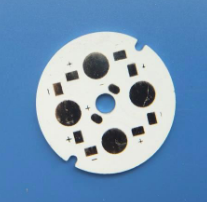
Ceramic pcb thickness
Importance Of Ceramic PCB Thickness In High-Frequency Applications
When it comes to high-frequency applications, the thickness of ceramic PCBs (Printed Circuit Boards) is a crucial factor that can significantly impact performance. You might be wondering why this is the case. Well, let’s dive into the nitty-gritty of why ceramic PCB thickness matters so much in these specialized applications.
First off, ceramic PCBs are known for their excellent thermal conductivity and electrical insulation properties.
These characteristics make them ideal for high-frequency applications, where managing heat and ensuring signal integrity are paramount. However, the thickness of the ceramic material can either enhance or hinder these benefits. For instance, a thicker ceramic layer can provide better heat dissipation, which is essential for components that generate a lot of heat. On the flip side, if the ceramic layer is too thick, it can introduce unwanted capacitance and inductance, which can distort high-frequency signals.
Transitioning to another important aspect, let’s talk about signal integrity.
In high-frequency applications, maintaining signal integrity is like walking a tightrope. Any deviation can lead to signal loss or interference, which can be catastrophic in applications like telecommunications or radar systems. The thickness of the ceramic PCB plays a pivotal role here. A thinner ceramic layer can reduce the distance that signals need to travel, thereby minimizing the chances of signal degradation. However, if the layer is too thin, it might not provide adequate insulation, leading to potential short circuits or signal crosstalk.
Moreover, the mechanical strength of the PCB is another factor influenced by its thickness.
High-frequency applications often involve complex and sensitive components that require a stable and robust platform. A thicker ceramic PCB can offer better mechanical support, reducing the risk of damage during manufacturing or operation. But again, there’s a trade-off. A thicker board can be more challenging to work with, especially when it comes to drilling holes for vias or mounting components. This can increase manufacturing costs and complexity, which is something to consider if you’re working on a budget.
Now, let’s not forget about the role of dielectric constant in high-frequency applications.
The dielectric constant of the ceramic material affects how signals propagate through the PCB. A higher dielectric constant can slow down signal transmission, which might be beneficial in some cases but detrimental in others. The thickness of the ceramic layer can influence this dielectric constant, adding another layer of complexity to the design process. Engineers often have to strike a balance between achieving the desired dielectric properties and maintaining the optimal thickness for thermal and mechanical performance.
In addition, the manufacturing process itself can be affected by the thickness of the ceramic PCB.
Thicker boards may require more advanced techniques and equipment, which can drive up production costs and lead times. On the other hand, thinner boards might be easier and cheaper to produce but could compromise on performance and durability. Therefore, it’s essential to consider the specific requirements of your high-frequency application when deciding on the thickness of your ceramic PCB.
In conclusion, the thickness of ceramic PCBs is a critical factor that can influence various aspects of high-frequency applications, from thermal management and signal integrity to mechanical strength and dielectric properties. While it might be tempting to opt for a one-size-fits-all approach, the reality is that each application has its unique set of requirements. By carefully considering these factors, you can make an informed decision that balances performance, cost, and manufacturability, ensuring that your high-frequency application runs smoothly and efficiently.

How Ceramic PCB Thickness Affects Thermal Management
When it comes to the world of electronics, thermal management is a crucial aspect that can make or break the performance of a device. One of the key players in this arena is the ceramic PCB, or printed circuit board. These boards are known for their excellent thermal conductivity, which makes them ideal for high-power applications. However, an often-overlooked factor that significantly impacts thermal management is the thickness of the ceramic PCB. Let’s dive into how ceramic PCB thickness affects thermal management and why it matters.
First off, it’s essential to understand that ceramic PCBs are made from materials like aluminum oxide, aluminum nitride, and beryllium oxide.
These materials are chosen for their superior thermal properties compared to traditional FR4 boards. The thickness of the ceramic layer can vary, and this variation plays a pivotal role in how heat is dissipated from the components mounted on the board.
Thicker ceramic PCBs generally offer better thermal management.
This is because a thicker ceramic layer can absorb and dissipate more heat. Imagine you’re cooking a steak; a thicker pan will distribute the heat more evenly, preventing any hot spots. Similarly, a thicker ceramic PCB can spread the heat generated by electronic components more uniformly, reducing the risk of overheating and potential failure.
However, it’s not just about slapping on a thicker layer and calling it a day.
There are trade-offs to consider. For one, thicker ceramic PCBs can be more expensive to manufacture. The cost of materials and the complexity of the production process can add up, making it a less economical choice for some applications. Additionally, a thicker board can be heavier and bulkier, which might not be suitable for devices where size and weight are critical factors.
On the flip side, thinner ceramic PCBs are lighter and more cost-effective.
They are easier to integrate into compact devices, making them a popular choice for consumer electronics. But here’s the catch: thinner boards have less material to absorb and dissipate heat. This can lead to higher temperatures around the components, which might necessitate additional cooling solutions like heat sinks or fans. These extra components can add to the overall cost and complexity of the device, somewhat negating the initial savings from using a thinner board.
Another aspect to consider is the thermal cycling performance.
Thicker ceramic PCBs tend to have better thermal cycling capabilities. This means they can withstand more cycles of heating and cooling without degrading. In applications where the device is subject to frequent temperature changes, a thicker board can offer better long-term reliability.
So, how do you strike the right balance? It ultimately depends on the specific requirements of your application.
For high-power applications like LED lighting, power electronics, and RF modules, a thicker ceramic PCB might be the way to go. The improved thermal management can enhance performance and reliability, justifying the higher cost and potential increase in size and weight. On the other hand, for consumer electronics where space and cost are at a premium, a thinner ceramic PCB might be more appropriate, provided that additional cooling solutions are in place.
In conclusion, the thickness of a ceramic PCB is a critical factor that affects thermal management. While thicker boards offer better heat dissipation and reliability, they come with higher costs and potential size constraints. Thinner boards are more economical and easier to integrate into compact devices but may require additional cooling measures. Understanding these trade-offs can help you make an informed decision that best suits your specific needs.
Comparing Ceramic PCB Thickness For Different Electronic Devices
When it comes to electronic devices, the thickness of ceramic PCBs (Printed Circuit Boards) can make a world of difference. You might not think about it much, but the thickness of these boards can impact everything from performance to durability. So, let’s dive into the nitty-gritty of comparing ceramic PCB thickness for different electronic devices and see why it matters.
First off, let’s talk about why ceramic PCBs are even a thing.
Unlike traditional PCBs made from materials like FR4, ceramic PCBs offer superior thermal conductivity and mechanical strength. This makes them ideal for high-power applications and environments where heat dissipation is crucial. But, as with anything, there’s no one-size-fits-all solution. The thickness of the ceramic PCB can vary depending on the specific needs of the device it’s being used in.
For instance, in high-frequency applications like RF (Radio Frequency) and microwave circuits, thinner ceramic PCBs are often preferred.
The reason is simple: thinner boards have lower dielectric losses, which means better signal integrity. In these cases, you might see ceramic PCBs with thicknesses as low as 0.25mm. This thin profile helps in maintaining the high-speed performance that these applications demand.
On the other hand, when it comes to power electronics, thicker ceramic PCBs are usually the go-to choice.
Devices like power amplifiers and LED modules generate a lot of heat, and thicker boards can handle this better. A thickness of around 1.0mm to 1.5mm is common in these applications. The added thickness provides better heat dissipation, ensuring that the device remains cool and operates efficiently. Plus, the mechanical strength of a thicker board can withstand the stresses that come with high-power applications.
Transitioning to consumer electronics, the story changes a bit.
Devices like smartphones and tablets require a balance between performance and form factor. Here, the thickness of the ceramic PCB is often a compromise between the two. Typically, you’ll find ceramic PCBs in the range of 0.5mm to 0.8mm. This thickness is enough to provide good thermal management without making the device bulky. After all, no one wants a smartphone that feels like a brick in their pocket.
Moreover, in automotive electronics, the requirements can be quite diverse.
For instance, in engine control units (ECUs), thicker ceramic PCBs are preferred due to the harsh operating conditions. These boards need to withstand high temperatures and vibrations, so a thickness of around 1.5mm is often used. Conversely, in infotainment systems, where the thermal and mechanical demands are not as extreme, thinner boards around 0.8mm might be sufficient.
It’s also worth mentioning that the manufacturing process can influence the choice of thickness.
Thicker ceramic PCBs are generally more robust and easier to handle during production, reducing the risk of damage. However, they can also be more expensive due to the increased material costs. Therefore, manufacturers often have to strike a balance between performance, durability, and cost.
In summary, the thickness of ceramic PCBs varies widely depending on the application. High-frequency devices benefit from thinner boards for better signal integrity, while power electronics require thicker boards for improved heat dissipation and mechanical strength. Consumer electronics find a middle ground to balance performance and form factor, and automotive applications have their own set of requirements based on the specific use case. Understanding these nuances can help in making informed decisions when designing or selecting ceramic PCBs for different electronic devices.
Advances In Manufacturing Techniques For Varying Ceramic PCB Thickness
When it comes to the world of electronics, ceramic PCBs are like the unsung heroes, quietly ensuring that everything runs smoothly. These little powerhouses are known for their excellent thermal conductivity, high mechanical strength, and impressive electrical insulation. But what really makes them stand out is their versatility in thickness, which can be a game-changer for various applications. Thanks to recent advances in manufacturing techniques, we now have more control over the thickness of ceramic PCBs than ever before.
First off, let’s talk about why thickness matters.
In the realm of electronics, the thickness of a PCB can significantly impact its performance. Thicker PCBs are generally more robust and can handle higher power loads, making them ideal for heavy-duty applications like power electronics and automotive systems. On the flip side, thinner PCBs are lighter and more flexible, which is perfect for compact devices like smartphones and wearable tech. So, having the ability to fine-tune the thickness of ceramic PCBs opens up a world of possibilities.
One of the most exciting advancements in this area is the development of new materials and composites.
Traditional ceramic PCBs are made from materials like alumina and aluminum nitride, which are great but have their limitations. Researchers are now experimenting with advanced composites that offer better performance and more flexibility in terms of thickness. For instance, some new materials can be layered to create multi-thickness PCBs, which can be customized for specific applications. This is a big deal because it means we can now design PCBs that are tailor-made for their intended use, rather than relying on a one-size-fits-all approach.
Another game-changer is the advent of precision manufacturing techniques.
Traditional methods like screen printing and tape casting have been around for a while, but they don’t offer the level of precision needed for today’s high-tech applications. Enter techniques like laser machining and 3D printing. These methods allow for incredibly precise control over the thickness of ceramic PCBs, down to the micrometer level. This level of precision is crucial for applications that require exact specifications, such as medical devices and aerospace technology.
Moreover, these advanced manufacturing techniques are not just about precision; they’re also about efficiency.
Traditional methods can be time-consuming and labor-intensive, which drives up costs. In contrast, modern techniques like 3D printing are much faster and more cost-effective. This means that manufacturers can produce high-quality ceramic PCBs at a lower cost, making them more accessible for a wider range of applications. It’s a win-win situation: better performance at a lower price.
Of course, no discussion about advances in manufacturing would be complete without mentioning sustainability.
The electronics industry is under increasing pressure to reduce its environmental footprint, and ceramic PCBs are no exception. Fortunately, many of the new materials and techniques being developed are more eco-friendly than their traditional counterparts. For example, some new composites are made from recycled materials, and advanced manufacturing methods often produce less waste. This is great news for both the industry and the planet.
In summary, the ability to vary the thickness of ceramic PCBs has come a long way, thanks to advances in materials and manufacturing techniques. Whether it’s through the use of new composites, precision methods like laser machining and 3D printing, or a focus on sustainability, the future looks bright for ceramic PCBs. So, the next time you marvel at the sleek design of your smartphone or the robust performance of your car’s electronics, take a moment to appreciate the tiny ceramic PCB working behind the scene


