China high speed pcb layout
Innovations In High-Speed PCB Layout Design In China
In recent years, China has emerged as a global leader in the field of high-speed printed circuit board (PCB) layout design, driven by rapid technological advancements and a robust manufacturing infrastructure. The country’s focus on innovation and efficiency has propelled it to the forefront of the electronics industry, where high-speed PCBs play a crucial role in the performance of modern electronic devices. As the demand for faster and more reliable electronic products continues to grow, Chinese companies are investing heavily in research and development to push the boundaries of PCB technology.
One of the key innovations in high-speed PCB layout design in China is the integration of advanced materials and manufacturing techniques.
Chinese engineers are increasingly utilizing high-frequency laminates and low-loss materials to enhance signal integrity and reduce electromagnetic interference. These materials are essential for maintaining the performance of high-speed circuits, especially in applications such as telecommunications, data centers, and consumer electronics. By adopting these cutting-edge materials, Chinese manufacturers are able to produce PCBs that meet the stringent requirements of high-speed applications.
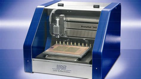
Moreover, the use of sophisticated design software has become a cornerstone of high-speed PCB layout design in China.
Advanced simulation tools allow engineers to model and analyze complex circuits with precision, ensuring optimal performance before the manufacturing process begins. These tools enable designers to identify potential issues such as signal reflection, crosstalk, and power integrity problems, which are critical in high-speed applications. By addressing these challenges early in the design phase, Chinese companies can reduce the risk of costly revisions and accelerate time-to-market for new products.
In addition to material and software innovations, China is also making strides in the miniaturization of high-speed PCBs.
As electronic devices become smaller and more compact, the need for miniaturized components and densely packed circuits has become increasingly important. Chinese manufacturers are leveraging advanced fabrication techniques, such as laser drilling and precision etching, to create PCBs with finer traces and smaller vias. This miniaturization not only enhances the performance of high-speed circuits but also allows for greater design flexibility and integration of additional features.
Furthermore, the collaborative ecosystem in China plays a significant role in driving innovation in high-speed PCB layout design.
The close proximity of component suppliers, manufacturers, and research institutions fosters a dynamic environment where ideas can be rapidly exchanged and implemented. This collaborative approach enables Chinese companies to stay at the cutting edge of technology and respond quickly to market demands. By working together, stakeholders in the PCB industry can develop new solutions that address the challenges of high-speed design and manufacturing.
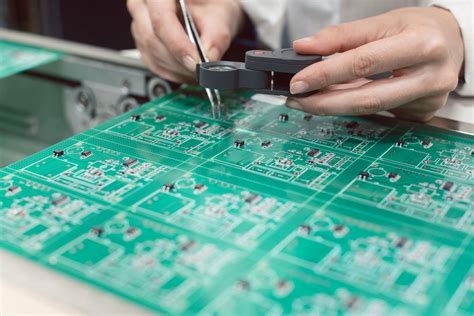
Finally, the emphasis on quality control and testing in China ensures that high-speed PCBs meet international standards and customer expectations.
Rigorous testing procedures, including signal integrity analysis and thermal management assessments, are conducted to verify the performance and reliability of PCBs. This commitment to quality not only enhances the reputation of Chinese manufacturers but also builds trust with global clients who rely on these high-speed solutions for their critical applications.
In conclusion, China’s advancements in high-speed PCB layout design are a testament to the country’s dedication to innovation and excellence in the electronics industry. Through the integration of advanced materials, sophisticated design software, miniaturization techniques, and a collaborative ecosystem, Chinese companies are setting new benchmarks in high-speed PCB technology. As the demand for faster and more efficient electronic devices continues to rise, China’s role as a leader in high-speed PCB design is poised to grow even further, shaping the future of the global electronics landscape.
Challenges And Solutions In Chinese High-Speed PCB Manufacturing
In the realm of modern electronics, the demand for high-speed printed circuit boards (PCBs) has surged, driven by the rapid advancement of technology and the need for faster, more efficient electronic devices. China, as a global leader in electronics manufacturing, plays a pivotal role in the production of high-speed PCBs. However, this sector is not without its challenges. Understanding these challenges and exploring potential solutions is crucial for maintaining China’s competitive edge in the global market.
One of the primary challenges in high-speed PCB manufacturing in China is the complexity of the design process.
High-speed PCBs require precise layout designs to ensure signal integrity and minimize electromagnetic interference. The intricate nature of these designs demands advanced software tools and highly skilled engineers. However, the availability of such resources can be limited, leading to potential bottlenecks in the design phase. To address this, Chinese manufacturers are increasingly investing in training programs to enhance the skills of their workforce and adopting cutting-edge design software to streamline the design process.
Moreover, material selection poses another significant challenge.
High-speed PCBs require materials with specific electrical properties to support high-frequency signals. The availability and cost of these specialized materials can vary, impacting the overall production cost and timeline. To mitigate this issue, Chinese manufacturers are exploring alternative materials that offer similar performance characteristics at a lower cost. Additionally, establishing strong relationships with reliable suppliers ensures a steady supply of high-quality materials, thereby reducing production delays.
In addition to design and material challenges, manufacturing high-speed PCBs involves stringent quality control measures.
The precision required in the fabrication process necessitates advanced manufacturing equipment and techniques. Any deviation from the specified parameters can result in defective products, leading to increased waste and higher production costs. To overcome this, Chinese manufacturers are adopting automated manufacturing processes and implementing rigorous quality control protocols. These measures not only enhance production efficiency but also ensure that the final products meet the required standards.
Furthermore, the rapid pace of technological advancements presents a continuous challenge for high-speed PCB manufacturers in China.
Keeping up with the latest trends and innovations is essential to remain competitive. This requires ongoing research and development efforts to integrate new technologies into the manufacturing process. Chinese companies are increasingly collaborating with research institutions and investing in R&D to stay at the forefront of technological advancements. By fostering a culture of innovation, they can adapt to changing market demands and maintain their leadership position.
Finally, environmental concerns are becoming increasingly important in the manufacturing sector, including high-speed PCB production.
The use of hazardous materials and the generation of electronic waste pose significant environmental challenges. To address these issues, Chinese manufacturers are adopting sustainable practices, such as using eco-friendly materials and implementing recycling programs. These initiatives not only reduce the environmental impact but also align with global sustainability goals, enhancing the reputation of Chinese manufacturers on the international stage.
In conclusion, while the challenges in Chinese high-speed PCB manufacturing are multifaceted, they are not insurmountable. Through strategic investments in technology, workforce development, and sustainable practices, China can continue to lead in this critical sector. By addressing these challenges head-on, Chinese manufacturers can ensure the production of high-quality, high-speed PCBs that meet the demands of the global market, thereby solidifying their position as a key player in the electronics industry.
The Role Of Advanced Software In China’s High-Speed PCB Layout
In recent years, China’s rapid advancements in technology have positioned it as a global leader in the electronics manufacturing industry. A critical component of this success is the development and implementation of high-speed printed circuit board (PCB) layouts. These layouts are essential for the efficient functioning of modern electronic devices, which demand faster processing speeds and greater data handling capabilities. At the heart of this technological evolution is the role of advanced software, which has become indispensable in the design and optimization of high-speed PCBs.
The complexity of high-speed PCB layouts necessitates the use of sophisticated software tools that can handle intricate design requirements.
These tools are designed to address various challenges, such as signal integrity, power distribution, and thermal management, which are crucial for the performance and reliability of electronic devices. By leveraging advanced algorithms and simulation capabilities, these software solutions enable engineers to predict and mitigate potential issues before they arise in the physical prototype stage. This predictive capability not only reduces the time and cost associated with PCB development but also enhances the overall quality and performance of the final product.
Moreover, the integration of artificial intelligence (AI) and machine learning (ML) into PCB design software has further revolutionized the industry.
AI-driven tools can analyze vast amounts of data to identify patterns and optimize design parameters, leading to more efficient and innovative solutions. For instance, AI can assist in automating the placement of components on a PCB, ensuring optimal signal paths and minimizing electromagnetic interference. This level of automation not only accelerates the design process but also reduces the likelihood of human error, which can be costly and time-consuming to rectify.
In addition to AI and ML, the use of cloud-based platforms has also transformed the landscape of high-speed PCB layout design in China.
These platforms facilitate collaboration among engineers, allowing them to work together seamlessly, regardless of their geographical location. By providing a centralized repository for design files and data, cloud-based solutions ensure that all team members have access to the most up-to-date information, thereby enhancing communication and reducing the risk of errors. Furthermore, cloud computing offers scalable resources that can handle the computational demands of complex simulations, making it an ideal solution for high-speed PCB design.
The role of advanced software in China’s high-speed PCB layout is not limited to design and simulation.
It also extends to the manufacturing process, where software tools are used to optimize production workflows and ensure quality control. For example, computer-aided manufacturing (CAM) software can generate precise instructions for automated machinery, ensuring that PCBs are produced with high accuracy and consistency. Additionally, real-time monitoring systems can track production metrics and identify potential issues, allowing for immediate corrective actions to be taken.
In conclusion, the integration of advanced software into the high-speed PCB layout process has been a driving force behind China’s success in the electronics manufacturing sector. By harnessing the power of AI, cloud computing, and other cutting-edge technologies, Chinese engineers are able to design and produce PCBs that meet the ever-increasing demands of modern electronic devices. As the industry continues to evolve, the role of advanced software will undoubtedly remain a critical factor in maintaining China’s competitive edge on the global stage.

Future Trends In China’s High-Speed PCB Technology
China’s high-speed PCB (Printed Circuit Board) technology has been at the forefront of the electronics manufacturing industry, driven by the country’s rapid advancements in technology and infrastructure. As the demand for faster and more efficient electronic devices continues to grow, the future trends in China’s high-speed PCB technology are poised to shape the global electronics landscape.
One of the most significant trends is the increasing integration of advanced materials and innovative design techniques.
High-speed PCBs require materials that can support faster signal transmission while minimizing signal loss and interference. In response, Chinese manufacturers are investing in research and development to explore new materials such as low-loss laminates and high-frequency substrates. These materials are crucial for maintaining signal integrity in high-speed applications, and their adoption is expected to become more widespread in the coming years.
Moreover, the miniaturization of electronic components is another trend that is influencing high-speed PCB design in China.
As devices become smaller and more compact, the need for PCBs that can accommodate these miniaturized components without compromising performance is paramount. This has led to the development of multi-layer PCBs and advanced fabrication techniques that allow for higher component density and more complex circuit designs. Consequently, Chinese manufacturers are focusing on enhancing their capabilities in producing multi-layer and high-density interconnect (HDI) PCBs to meet the demands of modern electronic devices.
In addition to material and design innovations, the adoption of automation and smart manufacturing processes is transforming the high-speed PCB industry in China.
The integration of artificial intelligence and machine learning in PCB design and manufacturing processes is enabling manufacturers to optimize production efficiency and reduce errors. By leveraging these technologies, Chinese companies can produce high-quality PCBs at a faster rate, thereby meeting the increasing demand for high-speed electronic components. This shift towards automation is expected to continue, with more manufacturers investing in smart factories and digitalization to enhance their competitive edge.
Furthermore, the rise of 5G technology is playing a pivotal role in shaping the future of high-speed PCB technology in China.
As 5G networks become more prevalent, the demand for PCBs that can support higher frequencies and faster data transmission rates is increasing. Chinese manufacturers are at the forefront of developing PCBs that are compatible with 5G technology, focusing on improving signal integrity and reducing electromagnetic interference. This trend is likely to accelerate as 5G technology becomes more widespread, driving further innovation in high-speed PCB design and manufacturing.
Lastly, the emphasis on sustainability and environmental responsibility is becoming increasingly important in the high-speed PCB industry.
Chinese manufacturers are adopting eco-friendly practices and materials to reduce the environmental impact of PCB production. This includes the use of lead-free soldering techniques, recycling of PCB materials, and the implementation of energy-efficient manufacturing processes. As global awareness of environmental issues continues to grow, the adoption of sustainable practices in PCB manufacturing is expected to become a standard requirement, further influencing the future trends in China’s high-speed PCB technology.
In conclusion, the future of high-speed PCB technology in China is characterized by advancements in materials, design, automation, 5G compatibility, and sustainability. These trends are not only shaping the domestic market but also positioning China as a leader in the global electronics industry. As technology continues to evolve, China’s high-speed PCB industry is set to play a crucial role in driving innovation and meeting the demands of the next generation of electronic devices.