Circuit board heat dissipation method
1.High heat generation devices plus heat sinks and heat conducting plates
When there are a few devices on the PCB that generate a lot of heat (less than 3), a heat sink or heat pipe can be added to the heat generating device. When the temperature cannot be lowered, a heat sink with a fan can be used to enhance the heat dissipation effect. When there are a large number of heat generating devices (more than 3), a large heat dissipation cover (plate) can be used. It is a special heat sink customized according to the position and height of the heat generating device on the PCB board, or a large flat heat sink with different component height positions cut out. The heat dissipation cover is buckled on the component surface as a whole, and it contacts each component to dissipate heat. However, due to the poor height consistency of components during soldering, the heat dissipation effect is not good. Usually, a soft thermal phase change thermal pad is added to the component surface to improve the heat dissipation effect.
2.Heat dissipation through the PCB board itself
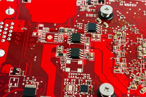
The widely used PCB board materials at present are copper-clad/epoxy glass cloth substrates or phenolic resin glass cloth substrates, and a small amount of paper-based copper-clad boards are used. Although these substrates have excellent electrical properties and processing properties, they have poor heat dissipation. As a heat dissipation path for high-heat components, it is almost impossible to expect the PCB resin to conduct heat, but to dissipate heat from the surface of the component to the surrounding air. However, as electronic products have entered the era of miniaturization, high-density installation, and high-heat assembly, it is not enough to rely solely on the surface of the component with a very small surface area to dissipate heat. At the same time, due to the large-scale use of surface-mounted components such as QFP and BGA, the heat generated by the components is transferred to the PCB board in large quantities. Therefore, the best way to solve the heat dissipation problem is to improve the heat dissipation capacity of the PCB itself that is in direct contact with the heat-generating components, and conduct or dissipate it through the PCB board.
3.Use reasonable routing design to achieve heat dissipation
Since the resin in the board has poor thermal conductivity, and the copper foil lines and holes are good conductors of heat, increasing the copper foil surplus rate and increasing the thermal conductive holes are the main means of heat dissipation.
To evaluate the heat dissipation capacity of the PCB, it is necessary to calculate the equivalent thermal conductivity (9eq) of the insulating substrate for PCB, a composite material composed of various materials with different thermal conductivities.
4.For equipment that uses free convection air cooling
it is best to arrange the integrated circuits (or other devices) in a longitudinal or horizontal manner.
5.The devices on the same printed circuit board should be arranged according to their heat generation and heat dissipation as much as possible.
Devices with low heat generation or poor heat resistance (such as small signal transistors, small-scale integrated circuits, electrolytic capacitors, etc.) are placed at the uppermost (inlet) of the cooling airflow, and devices with high heat generation or good heat resistance (such as power transistors, large-scale integrated circuits, etc.) are placed at the lowest downstream of the cooling airflow.
6.In the horizontal direction, high-power devices are arranged as close to the edge of the printed circuit board as possible to shorten the heat transfer path; in the vertical direction, high-power devices are arranged as close to the top of the printed circuit board as possible to reduce the impact of these devices on the temperature of other devices when they are working.
7.Devices that are sensitive to temperature are best placed in the lowest temperature area (such as the bottom of the device).
Never place it directly above the heating device. Multiple devices are best arranged in a staggered manner on the horizontal plane.
8.The heat dissipation of the printed circuit board in the equipment mainly depends on air flow
so when designing, it is necessary to study the air flow path and reasonably configure the components or printed circuit boards. When air flows, it always tends to flow to places with low resistance, so when configuring components on the printed circuit board, avoid leaving a large airspace in a certain area. The same problem should also be paid attention to the configuration of multiple printed circuit boards in the whole machine.
9.Avoid the concentration of hot spots on the PCB, distribute the power evenly on the PCB board as much as possible
and keep the surface temperature performance of the PCB uniform and consistent. It is often difficult to achieve strict uniform distribution during the design process, but it is necessary to avoid areas with too high power density to avoid overheating and affecting the normal operation of the entire circuit. If conditions permit, it is necessary to conduct thermal efficiency analysis of printed circuits. For example, the thermal efficiency index analysis software module added to some professional PCB design software can help designers optimize circuit design.
10.Arrange the devices with the highest power consumption and the highest heat generation near the best heat dissipation position.
Do not place devices with higher heat generation in the corners and edges of the printed circuit board unless there is a heat dissipation device near it. When designing power resistors, try to choose larger devices, and when adjusting the PCB layout, make sure there is enough heat dissipation space.
11.When connecting high heat dissipation devices to the substrate
the thermal resistance between them should be reduced as much as possible. In order to better meet the thermal characteristics requirements, some thermal conductive materials (such as applying a layer of thermal conductive silicone) can be used on the bottom of the chip, and a certain contact area should be maintained for the device to dissipate heat.
12.Connection between the device and the substrate:
(1) Try to shorten the length of the device lead;
(2) When selecting high-power devices, the thermal conductivity of the lead material should be considered, and try to select the device with the largest cross-section of the lead;
(3) Select a device with a large number of pins.
13.Device package selection:
(1) When considering thermal design, pay attention to the device package instructions and its thermal conductivity;
(2) Consider providing a good thermal conduction path between the substrate and the device package;
(3) Avoid air partitions in the thermal conduction path. If there is such a situation, fill it with thermal conductive materials.