Circuit Board Principles What types of working layers does a circuit board include?
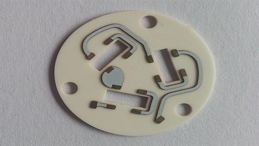
Circuit board can be called printed circuit board or printed circuit board. The English name is (Printed Circuit Board) PCB, (Flexible Printed Circuit board) FPC circuit board (FPC circuit board is also called flexible circuit board. Flexible circuit board is made of polyimide or polyester film as a substrate. It is a highly reliable and excellently flexible printed circuit board.
The names of circuit boards include: ceramic circuit board, alumina ceramic circuit board
, aluminum nitride ceramic circuit board, circuit board, PCB board, aluminum substrate, high-frequency board, thick copper board, impedance board, PCB, ultra-thin circuit board, ultra-thin circuit board, printed (copper etching technology) circuit board, etc.
The working principle of the circuit board: the surface copper foil conductive layer is separated by the board base insulating material, so that the current flows along the pre-designed route in various components to complete such as work, amplification, attenuation, modulation, demodulation, encoding, etc. Code and other functions.
On the most basic PCB, the parts are concentrated on one side and the wires are concentrated on the other side.
Because the wires only appear on one side, this PCB is called a single-sided board. Multilayer boards have wires on multiple layers, and there must be appropriate circuit connections between the two layers. This bridge between circuits is called a via. The basic design process of a circuit board can be divided into the following four steps:
(1) Design of circuit schematics—The design of circuit schematics is mainly to use the schematic editor of ProtelDXP to draw schematics.
(2) Generate network reports—The network report is a report that shows the connection relationship between the circuit principle and the various components in it
(3) It is a report that connects the circuit principle. The bridge and link between schematic design and circuit board design. Through the network report of the circuit schematic, the connection between components can be quickly found, thus facilitating the subsequent PCB design.
(3) Design of printed circuit board—The design of printed circuit board is what we usually call PCB design.
It is the final form of the circuit schematic. The related design of this part is more difficult than the design of the circuit schematic. We can use the powerful design function of ProtelDXP to complete this part of the design.
(4) Generate printed circuit board report—After the printed circuit board design is completed, various reports need to be generated, such as pin report, circuit board information report, network status report, etc. , and finally print out the printed circuit diagram.
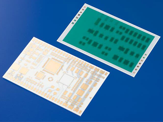
The green part is called solder mask, which is composed of resin and pigment.
The green one is green pigment, and there are also various other colors, which is no different from the paint for decoration. Before the assembly solder is printed on the circuit board, it is paste-like and flowable. After printing on the circuit board, it must be “cured” to allow the resin to harden by heat. The purpose of solder mask is to protect the circuit board from moisture, oxidation and dust. The only place not covered by solder mask is usually called pad, which is used for solder paste.
Generally, we choose green because green is less irritating to the eyes, and production and maintenance personnel are not prone to eye fatigue when staring at the PCB board for a long time. Commonly used colors include yellow, black and red. All kinds of colors are sprayed on the surface after manufacturing.
There is another reason. Because the commonly used color is green, the factory has the most spare green paint, so the cost of oil is relatively low.
Also, when repairing PCB boards, different wiring is easier to distinguish from white, while black and white are relatively difficult to see. In order to distinguish their own product levels, each factory uses two colors to distinguish high-end series from low-end series. For example, ASUS, a company that makes computer motherboards, has yellow boards for low-end and black boards for high-end. Biostar’s backboards are high-end and green boards are low-end.
The circuit board is mainly composed of pads, vias, mounting holes, wires, components, connectors, filling, electrical boundaries, etc. The main functions of each component are as follows:
Pads: metal holes for soldering component pins.
Vias: There are metal vias and non-metal vias, among which metal vias are used to connect component pins between layers.
Mounting holes: used to fix the circuit board.
Wires: electrical network copper films used to connect component pins.
Connectors: components used to connect between circuit boards.
Filling: copper coating used for ground network, which can effectively reduce impedance.
Electrical boundary: used to determine the size of the circuit board, and all components on the circuit board cannot exceed this boundary.
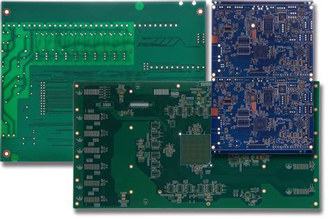
Circuit boards can be divided into three major categories according to the number of layers: single-sided boards, double-sided boards, and multi-layer circuit boards.
Multi-layer boards: refers to printed boards with more than three layers of conductive graphic layers and insulating materials in between, and the conductive graphics in between are interconnected as required. Multi-layer circuit boards are the product of the development of electronic information technology towards high speed, multi-function, large capacity, small size, thinness, and light weight.
Single-sided boards: On the most basic PCB, parts are concentrated on one side and wires are concentrated on the other side. Because the wires only appear on one side, this type of PCB is called a single-sided circuit board. Single-sided boards are usually simple to make and low in cost, but the disadvantage is that they cannot be applied to too complex products.
Double-sided boards: It is an extension of single-sided boards. When single-layer wiring cannot meet the needs of electronic products, double-sided boards must be used. Both sides have copper cladding and routing, and the lines between the two layers can be connected through vias to form the required network connection.
According to their characteristics, circuit boards can be divided into flexible circuit boards (FPC), rigid circuit boards (PCB), and flexible and rigid circuit boards (FPCB).
Circuit boards include many types of working layers, such as signal layers, protective layers, silk screen layers, internal layers, etc. The functions of various layers are briefly introduced as follows:
(1) Protective layer: mainly used to ensure that the places on the circuit board that do not need to be tinned are not tinned, thereby ensuring the reliability of the circuit board operation. Among them, Top Paste and Bottom Paste are the top solder mask layer and the bottom solder mask layer respectively; Top Solder and Bottom Solder are the solder paste protective layer and the bottom solder paste protective layer respectively.
(2) Signal layer: mainly used to place components or wiring. Protel DXP usually contains 30 middle layers, namely Mid Layer1~Mid Layer30. The middle layer is used to arrange signal lines, and the top and bottom layers are used to place components or copper.
(3) Silk screen layer: mainly used to print the serial number, production number, company name, etc. of components on the circuit board.
(4) Internal layer: mainly used as a signal routing layer. Protel DXP contains a total of 16 internal layers.
(5) Other layers: mainly include 4 types of layers.
Drill Guide: mainly used for the location of drilling holes on printed circuit boards.
Keep-Out Layer: mainly used to draw the electrical frame of the circuit board.
Drill Drawing: mainly used to set the drilling shape.
Multi-Layer: mainly used to set multi-layer.