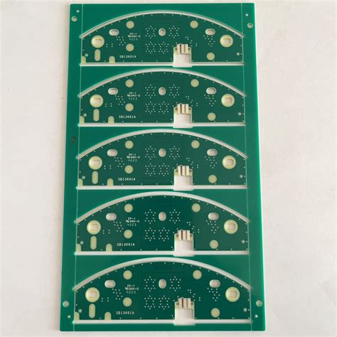
Common Mistakes in PCB Manufacturing Process and How to Avoid Them
Introduction
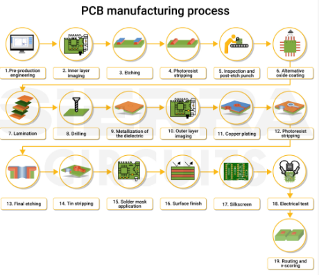
Printed Circuit Board (PCB) manufacturing is a complex process that requires precision and attention to detail at every stage. Even minor errors can lead to significant problems in the final product, affecting functionality, reliability, and performance. This article examines the most common mistakes that occur during PCB manufacturing, their potential consequences, and practical solutions to prevent them. By understanding these pitfalls, engineers, designers, and manufacturers can improve their PCB production quality and reduce costly rework.
1. Design-Related Mistakes
1.1 Incorrect Footprint Design
One of the most frequent errors in PCB design involves incorrect component footprints. This occurs when the pad sizes, spacing, or orientation don’t match the actual physical components.
Consequences:
- Components won’t fit properly during assembly
- Solder joint reliability issues
- Potential need for manual rework
Solutions:
- Always verify datasheet dimensions before creating footprints
- Use verified library components from reputable sources
- Create a physical prototype and test-fit components before full production
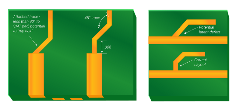
1.2 Insufficient Clearance and Creepage
Designers often underestimate the importance of proper clearance (air gap) and creepage (surface distance) between conductive elements.
Consequences:
- Risk of short circuits and arcing
- Potential safety hazards in high-voltage applications
- Non-compliance with industry standards
Solutions:
- Follow IPC-2221 standards for clearance and creepage requirements
- Use design rule checking (DRC) tools to verify spacing
- Consider voltage levels and environmental factors when determining spacing
1.3 Poor Thermal Management
Neglecting thermal considerations in PCB design can lead to overheating and premature failure.
Consequences:
- Component overheating and reduced lifespan
- Thermal stress leading to solder joint failures
- Performance degradation in sensitive circuits
Solutions:
- Incorporate proper thermal relief in pads
- Use thermal vias for heat dissipation
- Consider copper pours and heatsinks for high-power components
- Perform thermal analysis during design phase
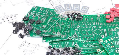
2. Manufacturing Process Errors
2.1 Improper Etching
Etching problems occur when too much or too little copper is removed from the board.
Common etching issues:
- Over-etching (thinner traces than designed)
- Under-etching (remaining copper causing shorts)
- Uneven etching across the board
Solutions:
- Maintain proper etchant concentration and temperature
- Control etching time precisely
- Use fresh etching solution and ensure proper agitation
- Implement automated optical inspection (AOI) after etching
2.2 Drilling Errors
Drilling mistakes can compromise the integrity of vias and through-hole components.
Common drilling problems:
- Misaligned holes
- Incorrect hole sizes
- Drill breakage causing damaged holes
- Burrs or rough hole edges
Solutions:
- Use high-quality drill bits and replace them regularly
- Maintain proper drill speed and feed rates
- Implement precise registration systems
- Conduct regular machine calibration
2.3 Solder Mask Application Issues
Solder mask protects copper traces from oxidation and prevents solder bridges, but application errors are common.
Common problems:
- Incomplete coverage leaving copper exposed
- Solder mask in pads (making soldering difficult)
- Uneven thickness
- Poor adhesion leading to peeling
Solutions:
- Ensure proper cleaning before solder mask application
- Control viscosity and curing parameters
- Use proper exposure and development processes
- Implement quality checks after application
3. Material Selection Mistakes
3.1 Choosing Wrong Substrate Material
Selecting inappropriate PCB substrate material can lead to performance issues.
Common material selection errors:
- Using standard FR-4 for high-frequency applications
- Selecting materials with inadequate thermal properties
- Choosing materials incompatible with the operating environment
Solutions:
- Understand application requirements (frequency, temperature, mechanical stress)
- Consult material datasheets and application notes
- Consider specialized materials for demanding applications
- Work with material suppliers for technical advice
3.2 Incorrect Copper Weight Selection
Choosing the wrong copper thickness can affect current carrying capacity and manufacturability.
Consequences:
- Excessive copper making fine traces difficult to etch
- Insufficient copper leading to overheating
- Impedance control challenges in high-speed designs
Solutions:
- Calculate current requirements and thermal considerations
- Balance copper weight with design complexity
- Consider stepped copper for mixed-current designs
- Consult manufacturing capabilities before finalizing design
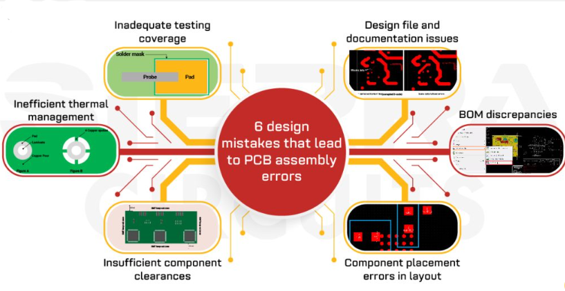
4. Quality Control Oversights
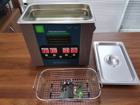
4.1 Inadequate Testing
Skipping or insufficient testing can allow defective boards to reach customers.
Common testing shortcomings:
- Relying solely on visual inspection
- Not performing electrical testing on all boards
- Incomplete functional testing
Solutions:
- Implement comprehensive testing protocols
- Use automated test equipment (ATE) for electrical testing
- Perform boundary scan testing for complex boards
- Establish sample testing procedures for production runs
4.2 Poor Documentation
Incomplete or inaccurate documentation leads to manufacturing errors.
Documentation issues:
- Missing or unclear assembly drawings
- Incomplete bill of materials (BOM)
- Unspecified tolerances or requirements
Solutions:
- Create comprehensive manufacturing packages
- Use standardized documentation formats
- Include all critical dimensions and specifications
- Verify documentation matches actual design files
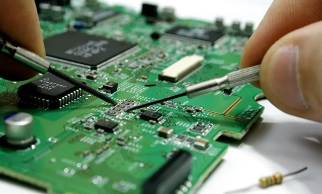
5. Assembly-Related Mistakes
5.1 Incorrect Stencil Design
Solder paste stencil problems lead to poor solder joint quality.
Common stencil issues:
- Wrong aperture sizes
- Improper stencil thickness
- Poor alignment during printing
Solutions:
- Calculate proper stencil thickness based on component types
- Optimize aperture designs for different components
- Implement fiducial markers for precise alignment
- Regularly clean and maintain stencils
5.2 Improper Reflow Profile
Incorrect reflow soldering parameters affect solder joint reliability.
Common reflow problems:
- Insufficient peak temperature
- Excessive time above liquidus
- Improper ramp rates causing thermal shock
Solutions:
- Develop profile based on solder paste specifications
- Consider component temperature limitations
- Use profile thermocouples to verify actual board temperatures
- Adjust profile for different board sizes and layouts
Conclusion
PCB manufacturing is a complex process with numerous opportunities for errors, but most common mistakes are preventable with proper knowledge and attention to detail. By understanding these potential pitfalls—from design through assembly—manufacturers can implement robust quality control measures and process improvements. Key strategies include thorough design verification, careful material selection, precise process control, and comprehensive testing. Investing in prevention ultimately saves time and costs associated with rework and field failures, while delivering higher quality, more reliable PCB products to customers.
As PCB technology continues to advance with higher densities and more complex requirements, maintaining vigilance against these common mistakes becomes even more critical. Continuous education, process optimization, and investment in quality assurance will separate successful PCB manufacturers from those struggling with preventable errors.