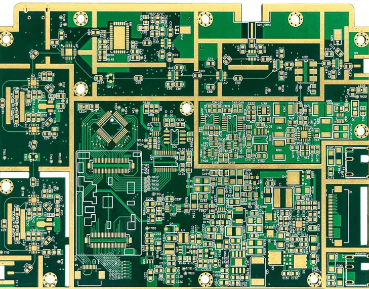
Common optimization methods for high-speed signals in PCB design
Take LVDS signal as an example to explain the common optimization methods for high-speed signals in PCB design:
LVDS (Low Voltage Differential Signaling) is a low-swing differential signal technology that enables signals to be transmitted at a rate of several hundred Mbps on differential PCB line pairs or balanced cables. Its low voltage amplitude and low current drive output achieve low noise and low power consumption.
LVDS signal is not only a differential signal, but also a high-speed digital signal.
Therefore, measures must be taken for the PCB line pairs used to transmit LVDS to prevent the signal from being reflected at the media terminal, and electromagnetic interference should be reduced to ensure the integrity of the signal. Some issues that need to be paid attention to when wiring PCB are as follows.
(1) Use a multi-layer board structure. Since LVDS signal is a high-speed signal, the layer adjacent to it should be the ground layer, and the LVDS signal should be shielded to prevent interference.
For boards with low density, if physical space conditions permit, it is best to place LVDS signal and other signals in different layers.

(2) Control the transmission line impedance. The impedance requirements of various differential lines are different.
According to the design requirements, the differential impedance and the corresponding line width spacing are calculated by the impedance meter software and set to the constraint manager. Differential lines reduce common mode interference by coupling with each other. When conditions permit, they should be routed in parallel as much as possible. There should be no vias or other signals between the two lines. The differential pair needs to strictly control the phase, so the length within the pair needs to be strictly controlled.
(3) Follow the principle of tight coupling.
When the two differential signal lines are very close, the current transmission direction is opposite, their magnetic fields cancel each other out, the electric fields couple with each other, and the electromagnetic radiation is much smaller. To reduce losses, ground vias can be added near the layer change holes when high-speed differential lines change layers.
(4) The routing should be as short and straight as possible.
The radiation intensity of the signal is proportional to the routing length of the signal line. The longer the high-frequency signal lead is, the easier it is to couple to the components close to it. Therefore, for high-frequency signal lines such as clocks, crystal oscillators, DDR data, LVDS lines, USB lines, HDMI lines, etc., the routing should be as short as possible. Avoid too many turns. It is best to use straight lines for high-frequency circuit wiring. If a turn is required, try to use 45° or arc lines at the turn to avoid 90° turns. This requirement is only used to improve the adhesion strength of copper foil in low-frequency circuits, but in high frequencies, meeting this requirement can reduce the external transmission of high-frequency signals and mutual coupling. The number of vias in the wiring and other factors that may cause line discontinuity should be minimized.

(5) The spacing between different differential line pairs cannot be too small.
LVDS has no restrictions on the choice of routing methods. Microstrip lines and strip lines are both acceptable, but it is important to have a good reference plane. The spacing between different differential line pairs cannot be too small and should be at least greater than the differential line spacing of 3 to 5 bits. If necessary, ground holes can be added between different differential line pairs to prevent crosstalk.
(6) LVDS signals should be kept away from other signals.
It is best to use different routing layers for LVDS signals and other signals, such as TTL signals. If the same layer of routing must be used due to design restrictions, the distance between LVDS routing and TTL routing should be far enough, at least greater than the differential line spacing of 3~5 bits.
(7) LVDS differential signals cannot be split across planes.
Although the two differential signals are return paths for each other, the split across the plane will not cut off the signal return, but the transmission line split across the plane will cause impedance discontinuity due to the lack of reference plane.
(8) The matching resistor at the receiving end should be as close to the receiving pin as possible, the distance should be as short as possible, and the wiring distance should also be as short as possible.
(9) Control the accuracy of the matching resistor.
The terminal matching resistor can be used to match the differential transmission line. Its resistance is generally between 90~130Ω. The circuit also needs this terminal matching resistor to generate a normal differential voltage. For point-to-point topology, the impedance of the routing is usually controlled at 100Ω, but the matching resistor can be adjusted according to the actual situation.
(10) Unused pin processing: All unused LVDS receiver input pins are left floating, all unused LVDS and TTL output pins are left floating, and all unused TTL transmit/driver input and control/


