Common Signs and Causes of PCB Failures: A Comprehensive Guide
Printed Circuit Boards (PCBs) are the backbone of modern electronics, found in everything from smartphones to industrial machinery. However, like any electronic component, PCBs can fail due to various reasons. Identifying the signs of PCB failure early can prevent costly repairs or complete system breakdowns. This article explores the most common signs of PCB failure, their underlying causes, and preventive measures.
Common Signs of PCB Failure
1. Physical Damage
Visible cracks, burns, or warping on a PCB are clear indicators of failure. Physical damage can result from:
- Mechanical stress (e.g., dropping a device)
- Excessive heat causing warping or delamination
- Chemical corrosion due to exposure to moisture or harsh environments
2. Component Burn Marks or Discoloration
Overheating often leads to burnt components or darkened areas on the PCB. This can be caused by:
- Short circuits
- Excessive current flow
- Poor thermal management (e.g., insufficient cooling)
3. Intermittent or Complete Failure
If a device works sporadically or stops functioning entirely, the PCB may have:
- Loose or broken connections
- Cold solder joints (poor soldering during manufacturing)
- Failed ICs or transistors
4. Unexpected Resets or Freezing
Frequent system crashes or reboots may indicate:
- Power supply issues (voltage fluctuations)
- Faulty capacitors (e.g., bulging or leaking electrolytic capacitors)
- Signal integrity problems (noise or crosstalk)
5. Poor Performance or Signal Degradation
Slow operation, data corruption, or weak signal output can result from:
- Impedance mismatches in high-frequency circuits
- Electromagnetic interference (EMI)
- Degraded traces or vias
Common Causes of PCB Failure
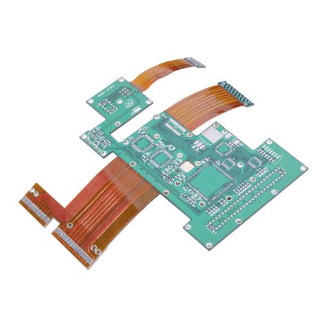
1. Manufacturing Defects
Even well-designed PCBs can fail due to production errors, such as:
- Poor soldering (cold joints, solder bridges)
- Incorrect component placement
- Contamination (dust, flux residues causing short circuits)
2. Environmental Factors
PCBs exposed to harsh conditions may fail due to:
- Moisture and humidity (leading to corrosion or dendritic growth)
- Extreme temperatures (thermal cycling causing expansion/contraction)
- Dust and debris (causing overheating or short circuits)
3. Electrical Overloads
Sudden power surges or incorrect voltage application can:
- Burn traces or components
- Cause dielectric breakdown in insulating layers
4. Aging and Wear
Over time, PCBs degrade due to:
- Electromigration (metal ions moving, causing open circuits)
- Thermal fatigue (repeated heating/cooling cycles weakening solder joints)
- Oxidation of contacts and traces
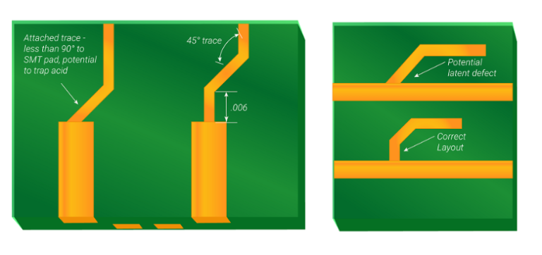
5. Poor Design Practices
Flaws in PCB design contribute to failures, including:
- Insufficient trace width (leading to overheating)
- Inadequate spacing between traces (causing short circuits)
- Lack of proper grounding (increasing EMI susceptibility)
Preventive Measures
To minimize PCB failures, consider the following best practices:
- Proper PCB design (following IPC standards for trace width, spacing, and thermal management)
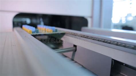
- Quality manufacturing (using automated optical inspection (AOI) and X-ray testing)
- Environmental protection (conformal coating, enclosures for moisture resistance)
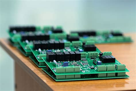
- Regular maintenance (cleaning, inspecting for early signs of failure)
Conclusion
PCB failures can stem from manufacturing defects, environmental stress, electrical issues, or poor design. Recognizing early warning signs—such as physical damage, overheating, or erratic behavior—helps prevent catastrophic failures. By adhering to robust design standards, quality manufacturing, and proper maintenance, PCB reliability can be significantly improved.
Understanding these common failure modes allows engineers and technicians to diagnose issues faster and implement effective solutions, ensuring longer-lasting and more reliable electronic systems.