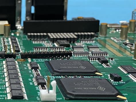
Comparison between electrical interconnection and optical interconnection of printed circuit boards
Optical interconnection structure principle of optoelectronic printed circuit boards
Optoelectronic printed circuit boards use high-speed optical connection technology to replace the copper wire connection currently used in computers, using photons instead of electrons as the medium to transmit data between circuit boards, chips and even various parts of chips. At the same time, it can also transmit traditional low-efficiency electrical signals. Its basic working principle is:
The electrical signal generated by the large-scale integrated chip is driven by the core surface acting VSCEL laser transmitter.
The laser beam is directly or through a lens transmitted to the polymer waveguide with a 45° mirror and reflected into the waveguide, and then transmitted to the PD through the other end of the waveguide mirror reflection, and then converted into an electrical signal through the receiving chip and transmitted to the large integrated chip. This enables high-speed communication between chips through optical waveguides, thereby improving the overall system performance. The production of this PCB is compatible with the traditional PCB production process, but the polymer waveguide is regarded as the copper property of the PCB.
II. Advantages of optical PCB
As mentioned earlier, the data transmission rate of copper wiring is affected by its parasitic resistance, inductance and capacitance. In the low frequency band, the series resistance and bypass capacitor of the circuit board have a great influence on the performance, directly determining the conversion time of the rising edge and the falling edge, thus affecting the data transmission rate; in the high frequency band, the influence of the series inductance of the connection exceeds the resistance, and the final result is the same as the series resistance and bypass capacitor, which limits the data transmission rate.
All these parasitic parameters depend largely on the geometry of the connection.
The resistance is proportional to the length of the connection and inversely proportional to the cross-sectional area. Therefore, the longer and thinner the connection, the lower the data transmission rate. The existing space restrictions will not allow the connection to be too thick. Although harder connections can be used to reduce the conversion time, the noise and power consumption are increased at the same time, and the increase in heat will be difficult to control.
Compared with electrical interconnection, optical interconnection has the following characteristics:
- The speed of optical interconnection is independent of the interconnection channel;
- Optical signals can propagate independently in space without interfering with each other;
- Optical signals can propagate in three-dimensional free space.
In addition, optical interconnection can be appropriately changed by spatial light modulator (SLM), and optical signals are very easy to convert into electrical signals.
In summary, the advantages of optical PCB and traditional PCB are compared as follows:
Traditional PCB Optoelectronic PCB
High energy consumption Less attenuation and dispersion, long transmission distance Low energy consumption
Interconnection density is subject to EMI Interconnection is not affected by EMI, no ground layer or reference plane
Low pin density (less than 50 pins/in) High pin density
Direct modulation or GHz carrier modulation THz carrier modulation
Small bandwidth Very large bandwidth
Difficult to control reflection Easy to control over-reflection
Three eras of optoelectronic PCB development
First generation: Dispersed fiber optical chip-chip interconnection and board-board interconnection on PCB
Developed in the early 1990s, mainly using discrete optical fiber and optical fiber connectors to exchange between modules or between modules and components, which is widely used by large mainframes. Due to its simple structure, it can provide relatively low-cost point-to-point optical connection.
Due to the use of single-film (Discretewww.pcbpc.org) optical fiber in the carrier board for optical interconnection, this form of optical interconnection is a derivative of the optical fiber communication technology that has been used in the past. Therefore, it is easier to realize the directional transmission mode of transmitting optical communication signals from one point to another.
The second generation: flexible substrate optical connection technology
Developed in the mid-1990s, the flexible substrate is used for optical fiber distribution. Similarly, this technology can be applied to the connectors mentioned above for point-to-point optical connection. The flexible optical waveguide sheet constitutes an optical signal network, which is the most prominent feature of the second development stage of the form and technology of optical waveguide circuit products. The metal wire is replaced by an optical fiber. So its characteristic is that the flexible material is used as a fixed carrier to realize the optical signal transmission of the flexible optical fiber. In terms of high-precision control of characteristic impedance in wiring, it has obvious improvements over the original electrical wiring form.
The third generation: hybrid optoelectronic connection technology
According to the characteristics of embedded materials and structures, it can be roughly divided into the following four technologies: surface polymer waveguide, embedded polymer waveguide, embedded optical fiber technology and embedded optical waveguide glass. The biggest difference from the first two is that this technology can provide multi-circuit optical waveguides and can be connected with active and passive components. The third generation of optical waveguide circuits is an optoelectronic printed circuit board that integrates the existing printed circuit board and the optical transmission line. The advantage of achieving this composite is that the board can have a higher wiring density of optical transmission lines than the optical fiber wiring form introduced in the early stage. At the same time, it also realizes the automated installation of photoelectric conversion components. The development trend of the materials used in the optical transmission path in the PCB adopts a polymer with low transmission loss and high heat resistance as the optical waveguide circuit material.


