Comprehensive Guide to PCB Via Design: Ensuring Signal Integrity and Reliability
Introduction
Printed Circuit Boards (PCBs) are the backbone of modern electronics, serving as the foundation for the interconnection and support of various electronic components. One of the critical elements in PCB design is the via, which provides electrical connections between different layers of the board. Proper via design is essential for ensuring signal integrity, thermal management, and overall reliability of the PCB. This article provides an in-depth exploration of PCB via design, covering its types, design considerations, manufacturing processes, and the latest trends in via technology.
1. Understanding PCB Vias
1.1. What is a Via?
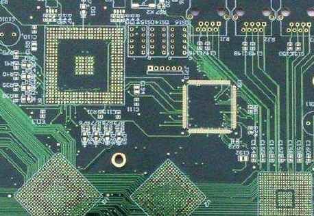
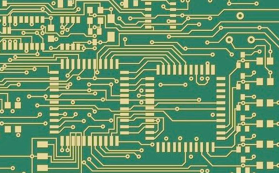
A via is a plated hole in a PCB that allows electrical connections to be made between different layers of the board. Vias are used to route signals, power, and ground between layers, enabling the creation of complex multilayer PCBs.
1.2. Types of Vias
There are several types of vias, each suited for different applications:
- Through-Hole Vias: These vias pass through the entire thickness of the PCB, connecting all layers. They are the most common type of via and are used in a wide range of applications.
- Blind Vias: These vias connect an outer layer to one or more inner layers but do not pass through the entire board. They are used in high-density interconnect (HDI) PCBs to save space.
- Buried Vias: These vias connect inner layers without reaching the outer layers. They are used in complex multilayer PCBs to increase routing density.
- Microvias: These are small vias, typically less than 150 microns in diameter, used in HDI PCBs. They can be blind or buried and are often stacked or staggered to connect multiple layers.
2. Design Considerations for PCB Vias
2.1. Signal Integrity
Signal integrity is a critical consideration in via design, especially for high-speed and high-frequency circuits.
- Impedance Matching: Vias can introduce impedance discontinuities, leading to signal reflections and degradation. Proper via design, including the use of controlled impedance vias, helps to minimize these effects.
- Stub Length: The stub length of a via (the unused portion of the via) can act as an antenna, causing signal reflections and EMI. Back-drilling or using blind and buried vias can reduce stub length and improve signal integrity.
- Via Placement: Proper placement of vias, considering signal paths and return paths, is essential for minimizing crosstalk and ensuring signal integrity.
2.2. Thermal Management
Vias play a crucial role in thermal management by providing a path for heat dissipation.
- Thermal Vias: These vias are used to transfer heat from components to the opposite side of the PCB or to internal copper planes. They are often filled with thermally conductive material to enhance heat transfer.
- Via Arrays: Arrays of thermal vias can be used under high-power components to spread heat and reduce thermal resistance.
- Via Size and Spacing: The size and spacing of thermal vias affect their thermal performance. Larger vias and closer spacing improve heat dissipation but must be balanced with manufacturing constraints.
2.3. Manufacturability
Designing vias that are manufacturable is essential for ensuring the reliability and cost-effectiveness of the PCB.
- Aspect Ratio: The aspect ratio (the ratio of via depth to diameter) affects the ease of plating and the reliability of the via. Higher aspect ratios are more challenging to manufacture and may require specialized processes.
- Via Filling: Filled vias, such as those filled with conductive or non-conductive material, can improve reliability and thermal performance but add complexity to the manufacturing process.
- Drilling and Plating: The precision of drilling and plating processes affects the quality of vias. Advanced techniques such as laser drilling and electroplating are used for high-density and microvia PCBs.
3. Via Design Guidelines
3.1. Via Size and Pad Diameter
The size of the via and the pad diameter are critical parameters in via design.
- Via Diameter: The via diameter should be chosen based on the current-carrying capacity and the manufacturing capabilities. Smaller vias are used in high-density designs, while larger vias are used for higher current paths.
- Pad Diameter: The pad diameter should be larger than the via diameter to ensure proper plating and mechanical strength. The pad size also affects the routing density and the ability to place components.
3.2. Via Placement and Routing
Proper placement and routing of vias are essential for minimizing signal integrity issues and ensuring efficient routing.
- Via Placement: Vias should be placed close to the components they connect to minimize trace length and reduce inductance. However, they should not be placed too close to avoid mechanical stress and soldering issues.
- Routing: Vias should be routed to minimize the number of layer transitions and reduce signal reflections. Differential pairs and high-speed signals should have matched via lengths to maintain signal integrity.
3.3. Via Stubs and Back-Drilling
Via stubs can cause signal reflections and degrade signal integrity, especially in high-speed designs.
- Stub Length: The stub length should be minimized to reduce its impact on signal integrity. Blind and buried vias can be used to eliminate stubs.
- Back-Drilling: Back-drilling is a process that removes the unused portion of the via stub, reducing its length and improving signal integrity. This technique is commonly used in high-speed and RF designs.
4. Advanced Via Technologies
4.1. Microvias
Microvias are small vias used in HDI PCBs to increase routing density and reduce board size.
- Laser Drilling: Microvias are typically drilled using laser technology, which allows for precise and small-diameter holes.
- Stacked and Staggered Vias: Microvias can be stacked (one on top of another) or staggered (offset from each other) to connect multiple layers. Stacked vias offer higher density but are more challenging to manufacture.
4.2. Filled Vias
Filled vias are used to improve thermal performance, mechanical strength, and reliability.
- Conductive Fill: Vias filled with conductive material, such as copper, enhance thermal conductivity and electrical performance.
- Non-Conductive Fill: Vias filled with non-conductive material, such as epoxy, improve mechanical strength and prevent solder wicking.
4.3. Via-in-Pad
Via-in-pad technology involves placing vias directly in the component pads, reducing the need for additional routing space.
- Advantages: Via-in-pad reduces the overall board size and improves signal integrity by minimizing trace length.
- Challenges: Via-in-pad requires precise manufacturing processes, such as via filling and planarization, to ensure a flat surface for component placement.
5. Latest Trends in Via Design
5.1. High-Speed and High-Frequency Design
As electronic devices continue to operate at higher speeds and frequencies, via design must evolve to meet the demands of signal integrity.
- Controlled Impedance Vias: These vias are designed to maintain consistent impedance, reducing signal reflections and degradation.
- Differential Pair Vias: Differential pairs require matched via lengths and placements to maintain signal integrity and minimize skew.
5.2. 3D Packaging and Integration
The trend towards 3D packaging and integration is driving the development of advanced via technologies.
- Through-Silicon Vias (TSVs): TSVs are used in 3D ICs to connect multiple layers of silicon, enabling higher density and performance.
- Interposer Vias: Interposers use vias to connect different chips and components in a 3D package, improving signal integrity and thermal management.
5.3. Additive Manufacturing
Additive manufacturing, or 3D printing, is emerging as a potential method for creating vias in PCBs.
- Flexibility: Additive manufacturing allows for the creation of complex via structures and custom designs.
- Rapid Prototyping: 3D printing enables rapid prototyping and testing of via designs, reducing development time.
6. Conclusion
PCB via design is a critical aspect of ensuring the performance, reliability, and manufacturability of electronic devices. Proper via design involves careful consideration of signal integrity, thermal management, and manufacturability, as well as adherence to design guidelines and standards. Advanced via technologies, such as microvias, filled vias, and via-in-pad, are driving innovation in PCB design, enabling higher density and performance. As the electronics industry continues to evolve, via design will play an increasingly important role in meeting the demands of high-speed, high-frequency, and 3D integrated circuits. By staying abreast of the latest trends and technologies in via design, engineers and designers can create PCBs that deliver superior performance and reliability.


