Copper Inlay PCB: Revolutionizing Printed Circuit Board Technology
Introduction
The evolution of printed circuit boards (PCBs) has been a cornerstone in the advancement of modern electronics. As devices become smaller, more powerful, and more complex, the demand for innovative PCB technologies has grown exponentially. One such innovation is the Copper Inlay PCB, a cutting-edge approach that combines traditional PCB manufacturing techniques with advanced materials and processes to enhance performance, reliability, and thermal management. This article delves into the concept of Copper Inlay PCBs, their manufacturing process, advantages, applications, and future prospects.
What is a Copper Inlay PCB?
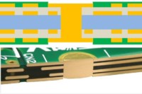
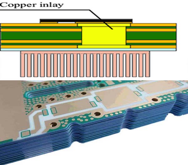
A Copper Inlay PCB is a specialized type of printed circuit board that incorporates embedded copper elements within the substrate material. Unlike traditional PCBs, where copper traces are etched onto the surface of the board, Copper Inlay PCBs feature copper elements that are precisely embedded into the board’s core or layers. These copper inlays can take various forms, such as pads, blocks, or even complex geometries, and are designed to improve thermal conductivity, electrical performance, and mechanical stability.
The copper inlays are typically embedded using advanced manufacturing techniques such as laser drilling, precision milling, or additive manufacturing. This allows for highly accurate placement and integration of copper elements within the PCB structure.
Manufacturing Process of Copper Inlay PCBs
The production of Copper Inlay PCBs involves several sophisticated steps, each critical to ensuring the final product’s quality and performance. Below is an overview of the key stages in the manufacturing process:
- Design and Simulation
The process begins with the design of the PCB layout using computer-aided design (CAD) software. Engineers simulate the thermal and electrical performance of the board to determine the optimal placement and size of the copper inlays. This step ensures that the inlays will effectively address thermal management and signal integrity requirements. - Substrate Preparation
The base substrate material, typically a high-performance laminate such as FR-4, polyimide, or ceramic-filled PTFE, is prepared. The substrate is cleaned and treated to ensure proper adhesion of the copper inlays. - Copper Inlay Integration
The copper inlays are precisely embedded into the substrate using advanced techniques such as laser ablation or CNC milling. These methods allow for the creation of cavities or grooves in the substrate, into which the copper elements are inserted. The inlays are then bonded to the substrate using high-temperature adhesives or soldering techniques. - Lamination and Layer Stacking
Once the copper inlays are in place, the PCB undergoes a lamination process. Multiple layers of substrate and copper foil are stacked and pressed together under high temperature and pressure. This step ensures a strong bond between the layers and the embedded copper elements. - Drilling and Plating
After lamination, the PCB is drilled to create vias and through-holes. These holes are then plated with copper to establish electrical connections between the layers. The copper inlays are also connected to the surrounding circuitry during this step. - Etching and Surface Finishing
The excess copper is etched away to define the final circuit pattern. The board is then coated with a surface finish, such as ENIG (Electroless Nickel Immersion Gold) or HASL (Hot Air Solder Leveling), to protect the copper traces and enhance solderability. - Testing and Quality Control
The finished Copper Inlay PCB undergoes rigorous testing to ensure it meets the required electrical, thermal, and mechanical specifications. Advanced testing methods such as thermal imaging, X-ray inspection, and electrical continuity testing are employed to verify the board’s performance.
Advantages of Copper Inlay PCBs
Copper Inlay PCBs offer several significant advantages over traditional PCBs, making them an attractive choice for high-performance applications. Some of the key benefits include:
- Enhanced Thermal Management
One of the primary advantages of Copper Inlay PCBs is their superior thermal conductivity. The embedded copper elements act as heat sinks, efficiently dissipating heat away from critical components. This is particularly beneficial in high-power applications such as power electronics, LED lighting, and automotive systems, where effective thermal management is essential to prevent overheating and ensure reliability. - Improved Electrical Performance
The integration of copper inlays can reduce electrical resistance and improve signal integrity. By embedding copper directly into the substrate, the distance between components and the copper traces is minimized, reducing parasitic inductance and capacitance. This results in faster signal transmission and lower power losses, making Copper Inlay PCBs ideal for high-frequency and high-speed applications. - Mechanical Stability
The embedded copper elements provide additional structural support to the PCB, enhancing its mechanical stability and durability. This is particularly important in applications subject to mechanical stress, vibration, or thermal cycling, such as aerospace and automotive electronics. - Space Efficiency
Copper Inlay PCBs enable more compact and lightweight designs by integrating thermal and electrical functions within the substrate. This reduces the need for external heat sinks or additional layers, allowing for smaller and more efficient electronic devices. - Design Flexibility
The ability to embed copper elements in precise locations and shapes offers greater design flexibility. Engineers can tailor the PCB’s thermal and electrical properties to meet the specific requirements of their application, resulting in optimized performance and reliability.
Applications of Copper Inlay PCBs
Copper Inlay PCBs are well-suited for a wide range of applications across various industries. Some of the most prominent applications include:
- Power Electronics
In power electronics, efficient thermal management is critical to ensuring the reliability and longevity of components such as power transistors, diodes, and voltage regulators. Copper Inlay PCBs are widely used in power supplies, inverters, and motor drives to dissipate heat effectively and maintain stable operation. - LED Lighting
High-power LED lighting systems generate significant amounts of heat, which can degrade performance and reduce lifespan. Copper Inlay PCBs are commonly used in LED modules and fixtures to provide efficient heat dissipation and ensure consistent light output. - Automotive Electronics
The automotive industry demands robust and reliable electronics capable of withstanding harsh operating conditions. Copper Inlay PCBs are used in engine control units (ECUs), battery management systems (BMS), and infotainment systems to enhance thermal performance and durability. - Aerospace and Defense
In aerospace and defense applications, electronics must operate reliably under extreme temperatures, vibrations, and mechanical stress. Copper Inlay PCBs are employed in avionics, radar systems, and satellite communications to ensure optimal performance and longevity. - Telecommunications
High-frequency and high-speed communication systems require PCBs with excellent signal integrity and thermal management. Copper Inlay PCBs are used in 5G infrastructure, RF amplifiers, and optical transceivers to meet these demanding requirements. - Medical Devices
Medical electronics, such as imaging systems and implantable devices, require compact and reliable PCBs with efficient thermal management. Copper Inlay PCBs are increasingly being adopted in these applications to enhance performance and patient safety.
Future Prospects of Copper Inlay PCBs
As the demand for high-performance electronics continues to grow, Copper Inlay PCBs are poised to play an increasingly important role in the industry. Several trends and developments are expected to drive the adoption of this technology in the coming years:
- Miniaturization
The trend toward smaller and more compact electronic devices will drive the need for advanced PCB technologies like Copper Inlay PCBs. Their ability to integrate thermal and electrical functions within the substrate makes them ideal for space-constrained applications. - 5G and Beyond
The rollout of 5G networks and the development of future communication technologies will require PCBs with superior thermal and electrical performance. Copper Inlay PCBs are well-positioned to meet these demands, enabling faster and more reliable communication systems. - Electric Vehicles (EVs)
The rapid growth of the electric vehicle market will create significant opportunities for Copper Inlay PCBs. Their ability to handle high power levels and provide efficient thermal management makes them ideal for EV powertrains, battery systems, and charging infrastructure. - Advanced Manufacturing Techniques
Ongoing advancements in manufacturing technologies, such as additive manufacturing and laser processing, will further enhance the capabilities of Copper Inlay PCBs. These techniques will enable more complex and precise copper inlays, opening up new possibilities for PCB design and performance. - Sustainability
As the electronics industry focuses on sustainability, Copper Inlay PCBs can contribute by reducing material waste and improving energy efficiency. Their ability to enhance thermal performance can also extend the lifespan of electronic devices, reducing electronic waste.
Conclusion
Copper Inlay PCBs represent a significant advancement in PCB technology, offering enhanced thermal management, improved electrical performance, and greater design flexibility. As the electronics industry continues to evolve, the demand for high-performance PCBs will only increase, making Copper Inlay PCBs a key enabler of future innovations. From power electronics and automotive systems to telecommunications and medical devices, the applications of Copper Inlay PCBs are vast and varied. With ongoing advancements in manufacturing techniques and materials, the potential for this technology is virtually limitless, paving the way for a new era of electronic design and performance.


