Custom pcb
Benefits Of Custom PCB Design For Electronics Projects
Custom printed circuit boards (PCBs) have become an integral component in the development of modern electronics projects, offering a multitude of benefits that enhance both the functionality and efficiency of electronic devices. As technology continues to advance, the demand for more sophisticated and compact electronic solutions has increased, making custom PCB design an essential consideration for engineers and developers.
One of the primary advantages of custom PCB design is the ability to tailor the board to meet specific project requirements.
Unlike generic PCBs, which may include unnecessary components or features, custom PCBs are designed with the exact specifications needed for a particular application. This customization ensures optimal performance and reliability, as the board is engineered to support the unique electrical and mechanical demands of the project.
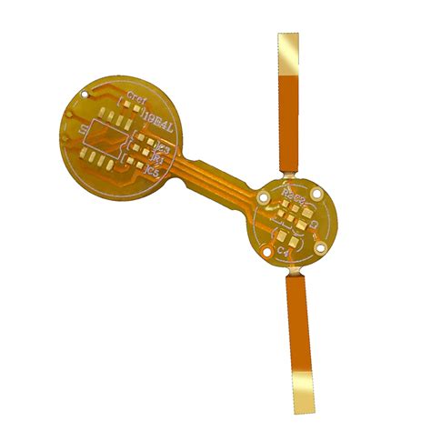
Moreover, custom PCBs contribute significantly to the miniaturization of electronic devices.
As consumer preferences shift towards smaller, more portable gadgets, the need for compact circuit solutions has become paramount. Custom PCBs allow for the integration of multiple functions into a single board, reducing the overall size and weight of the device.
This not only enhances the portability of the product but also improves its aesthetic appeal, making it more attractive to end-users. Additionally, the use of custom PCBs can lead to cost savings in the long run.
While the initial design and production of a custom PCB may require a higher investment compared to off-the-shelf solutions, the benefits of reduced material waste, improved efficiency, and fewer assembly errors can result in significant cost reductions over time.
By eliminating unnecessary components and streamlining the manufacturing process, custom PCBs can lower production costs and increase the profitability of electronic projects.
Furthermore, custom PCB design offers enhanced performance and reliability.
By optimizing the layout and component placement, engineers can minimize signal interference and improve the overall electrical performance of the device. This is particularly important in high-frequency applications, where even minor design flaws can lead to significant performance issues.
Custom PCBs also allow for better thermal management, as heat-generating components can be strategically placed to dissipate heat more effectively, thereby extending the lifespan of the device.
In addition to performance benefits, custom PCBs provide greater design flexibility.
Engineers have the freedom to experiment with different materials, shapes, and sizes, enabling them to create innovative solutions that meet the evolving needs of the market.
This flexibility is crucial in industries such as consumer electronics, automotive, and telecommunications, where rapid technological advancements require constant adaptation and innovation.
Moreover, custom PCBs facilitate easier troubleshooting and maintenance.
With a design tailored to the specific needs of the project, identifying and addressing issues becomes more straightforward. This can lead to faster repair times and reduced downtime, which is particularly beneficial in critical applications where reliability is paramount.
In conclusion, the benefits of custom PCB design for electronics projects are manifold, ranging from improved performance and reliability to cost savings and design flexibility.
As the demand for more advanced and compact electronic solutions continues to grow, custom PCBs will undoubtedly play a crucial role in shaping the future of technology.
By providing tailored solutions that meet the specific needs of each project, custom PCBs enable engineers to push the boundaries of innovation and deliver cutting-edge products that meet the ever-evolving demands of the market.
How To Choose The Right Materials For Your Custom PCB
When embarking on the journey of designing a custom printed circuit board (PCB), one of the most critical decisions you will face is selecting the appropriate materials. The choice of materials not only influences the performance and reliability of the PCB but also affects its cost and manufacturability. Therefore, understanding the various material options and their implications is essential for achieving a successful design.
To begin with, the substrate material forms the foundation of any PCB.
The most commonly used substrate is FR-4, a fiberglass-reinforced epoxy laminate. FR-4 is favored for its excellent balance of cost, mechanical strength, and electrical insulation properties. However, for applications requiring higher performance, such as high-frequency or high-temperature environments, alternative materials like polyimide or Rogers laminates may be more suitable. Polyimide offers superior thermal stability, making it ideal for aerospace and automotive applications, while Rogers materials provide low dielectric loss, which is crucial for high-frequency circuits.
In addition to the substrate, the choice of copper cladding is another vital consideration.
Copper is the standard conductive material used in PCBs due to its excellent electrical conductivity. The thickness of the copper layer, often referred to as copper weight, can vary depending on the current-carrying requirements of the circuit. Standard copper weights are typically 1 oz/ft², but for high-power applications, thicker copper layers may be necessary to handle increased current loads without overheating.
Furthermore, the solder mask material plays a significant role in protecting the copper traces from oxidation and preventing solder bridges during assembly.
The most common solder mask material is epoxy liquid photoimageable (LPI) solder mask, which offers good adhesion and chemical resistance. However, for applications requiring higher durability or specific color requirements, other options such as liquid photoimageable (LPI) solder mask or dry film solder mask may be considered.
Transitioning to the topic of surface finishes, these are applied to the exposed copper areas to enhance solderability and protect against corrosion.
The choice of surface finish can impact the assembly process and the long-term reliability of the PCB. Common surface finishes include Hot Air Solder Leveling (HASL), Electroless Nickel Immersion Gold (ENIG), and Organic Solderability Preservative (OSP). HASL is cost-effective and provides a robust solderable surface, but it may not be suitable for fine-pitch components due to its uneven surface. ENIG, on the other hand, offers a flat surface and excellent corrosion resistance, making it ideal for complex and high-reliability applications. OSP is an environmentally friendly option that provides a flat surface but may have a limited shelf life.
Finally, considering the environmental and regulatory requirements is crucial when selecting materials for a custom PCB.
Compliance with standards such as RoHS (Restriction of Hazardous Substances) ensures that the materials used do not contain harmful substances like lead or mercury. Additionally, for applications in specific industries, such as medical or military, adherence to industry-specific standards may be necessary.
In conclusion, choosing the right materials for your custom PCB involves a careful evaluation of the application’s requirements, performance criteria, and cost considerations. By understanding the properties and trade-offs of different materials, you can make informed decisions that will lead to a reliable and efficient PCB design.

The Future Of Custom PCB Manufacturing Technologies
The future of custom PCB (Printed Circuit Board) manufacturing technologies is poised for significant advancements, driven by the increasing demand for more efficient, compact, and versatile electronic devices. As the backbone of modern electronics, PCBs are integral to the functionality of a wide array of products, from consumer electronics to industrial machinery. Consequently, the evolution of PCB manufacturing technologies is crucial to meeting the ever-growing expectations of both consumers and industries.
One of the most promising developments in custom PCB manufacturing is the advent of additive manufacturing, commonly known as 3D printing.
This technology offers the potential to revolutionize the way PCBs are designed and produced. Unlike traditional subtractive methods, which involve etching away unwanted material from a solid substrate, additive manufacturing builds the circuit layer by layer. This approach not only reduces material waste but also allows for greater design flexibility. As a result, manufacturers can create more complex and compact circuit designs that were previously unattainable with conventional methods.
Moreover, the integration of advanced materials into PCB manufacturing is another area of significant progress.
The use of flexible substrates, such as polyimide and other polymers, enables the production of flexible PCBs that can be bent and folded without compromising their functionality. This innovation is particularly beneficial for applications in wearable technology and other compact devices where space is at a premium. Additionally, the incorporation of conductive inks and pastes, which can be printed onto various substrates, further enhances the versatility of PCB designs, allowing for the creation of circuits on unconventional surfaces.
In tandem with these material advancements, the implementation of artificial intelligence (AI) and machine learning in PCB design and manufacturing processes is set to transform the industry.
AI algorithms can optimize circuit layouts, predict potential design flaws, and even automate the entire design process, significantly reducing the time and cost associated with PCB production. Furthermore, machine learning can enhance quality control by identifying defects and inconsistencies in real-time, ensuring that only the highest quality products reach the market.
Another critical aspect of the future of custom PCB manufacturing is the push towards sustainability.
As environmental concerns continue to rise, the industry is under pressure to adopt greener practices. This includes the development of eco-friendly materials and processes that minimize the environmental impact of PCB production. For instance, water-based etching solutions and biodegradable substrates are being explored as alternatives to traditional, more harmful materials. Additionally, recycling initiatives are being implemented to recover valuable metals from discarded PCBs, reducing the need for virgin resources.
As we look to the future, it is clear that the convergence of these technologies will lead to a new era in custom PCB manufacturing.
The ability to produce highly customized, efficient, and sustainable PCBs will not only meet the demands of current applications but also pave the way for innovations in emerging fields such as the Internet of Things (IoT), autonomous vehicles, and advanced medical devices. In conclusion, the future of custom PCB manufacturing technologies is bright, with advancements in additive manufacturing, materials science, AI, and sustainability driving the industry towards unprecedented levels of innovation and efficiency. As these technologies continue to evolve, they will undoubtedly shape the landscape of electronics manufacturing for years to come.
Common Mistakes To Avoid In Custom PCB Prototyping
In the realm of electronics design, custom printed circuit boards (PCBs) are pivotal in transforming innovative ideas into functional prototypes. However, the journey from concept to prototype is fraught with potential pitfalls that can derail even the most promising projects. Understanding and avoiding common mistakes in custom PCB prototyping is essential for ensuring a smooth development process and achieving a successful outcome.
One of the most frequent errors in custom PCB prototyping is inadequate planning.
Designers often rush into the design phase without thoroughly understanding the project requirements or constraints. This oversight can lead to a cascade of issues, such as incorrect component selection or inappropriate board size, which can ultimately result in costly redesigns. To mitigate this risk, it is crucial to invest time in the initial planning stages, clearly defining the project scope, specifications, and constraints. This foundational step sets the stage for a more streamlined design process.
Transitioning from planning to design, another common mistake is neglecting design for manufacturability (DFM) principles.
Designers may focus solely on the functionality of the PCB, overlooking the practicalities of manufacturing. This can lead to designs that are difficult or expensive to produce. To avoid this, it is important to collaborate closely with manufacturers during the design phase, ensuring that the PCB layout adheres to industry standards and manufacturing capabilities. By doing so, designers can identify potential issues early and make necessary adjustments before the prototyping stage.
Furthermore, improper component placement and routing can significantly impact the performance and reliability of a custom PCB.
Designers often underestimate the importance of strategic component placement, which can lead to issues such as signal interference or thermal management problems. To address this, it is essential to follow best practices for component placement and routing, such as minimizing trace lengths and ensuring adequate spacing between components. Additionally, utilizing simulation tools can help identify potential issues and optimize the design before moving to the prototyping phase.
In addition to design-related mistakes, overlooking thorough testing and validation is a critical error that can compromise the functionality of a custom PCB.
Designers may assume that a successful design automatically translates to a functional prototype, but this is not always the case.
Comprehensive testing, including functional testing, signal integrity analysis, and thermal testing, is necessary to validate the design and ensure it meets the intended specifications. By prioritizing testing and validation, designers can identify and rectify issues before they escalate into more significant problems.
Moreover, communication breakdowns between design teams and manufacturers can lead to misunderstandings and errors in the prototyping process.
Clear and consistent communication is vital to ensure that all parties are aligned on the project requirements and expectations. Regular updates and feedback loops can help bridge any gaps and facilitate a more collaborative approach to prototyping.
Finally, failing to document the design and prototyping process is a mistake that can hinder future iterations and improvements.
Comprehensive documentation provides a valuable reference for future projects and helps maintain consistency across different design iterations. By meticulously documenting each step of the process, designers can create a knowledge base that supports continuous improvement and innovation.
In conclusion, while custom PCB prototyping presents numerous challenges, being aware of and avoiding common mistakes can significantly enhance the likelihood of success. Through careful planning, adherence to DFM principles, strategic component placement, thorough testing, effective communication, and diligent documentation, designers can navigate the complexities of custom PCB prototyping with confidence and precision.


