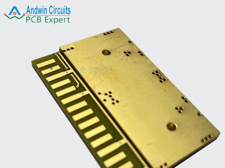
Customized heavy copper pcb
Benefits Of Custom Printed Circuit Boards In Modern Electronics
Custom printed circuit boards (PCBs) have become an integral component in the realm of modern electronics, offering a multitude of benefits that enhance both the functionality and efficiency of electronic devices.
As technology continues to advance at a rapid pace, the demand for more sophisticated and reliable electronic components has surged, making custom PCBs an essential element in the design and manufacturing process.
One of the primary advantages of custom PCBs is their ability to be tailored to specific requirements, allowing for greater flexibility in design.
This customization enables engineers to optimize the layout and functionality of the circuit board to meet the unique needs of a particular application, thereby improving the overall performance of the device.
Moreover, custom PCBs contribute significantly to the miniaturization of electronic devices.
As consumer demand shifts towards more compact and portable gadgets, the need for smaller yet more powerful components becomes paramount. Custom PCBs allow for the integration of multiple functions onto a single board, reducing the overall size and weight of the device without compromising on performance. This is particularly beneficial in industries such as telecommunications, medical devices, and consumer electronics, where space is often at a premium.
In addition to size reduction, custom PCBs also enhance the reliability and durability of electronic devices.
By designing a PCB specifically for a particular application, engineers can ensure that the board is capable of withstanding the environmental conditions and stresses it will encounter during its operational life. This tailored approach minimizes the risk of component failure, thereby extending the lifespan of the device and reducing maintenance costs. Furthermore, custom PCBs can be designed with specific materials and coatings that provide additional protection against factors such as moisture, heat, and electromagnetic interference, further enhancing their robustness.
Another significant benefit of custom PCBs is their contribution to improved signal integrity and performance.
By carefully designing the layout of the circuit board, engineers can minimize issues such as signal loss, crosstalk, and electromagnetic interference, which can adversely affect the performance of electronic devices. This is particularly important in high-frequency applications, where even minor disruptions can lead to significant performance degradation. Custom PCBs allow for precise control over the placement and routing of components, ensuring optimal signal paths and reducing the likelihood of performance issues.
Furthermore, custom PCBs offer cost advantages in the long run.
While the initial design and manufacturing process may be more expensive compared to standard off-the-shelf PCBs, the benefits of improved performance, reliability, and reduced size often result in cost savings over the lifecycle of the product. Additionally, custom PCBs can streamline the assembly process by reducing the number of components and connections required, leading to faster production times and lower labor costs.
In conclusion, the benefits of custom printed circuit boards in modern electronics are manifold
ranging from enhanced design flexibility and miniaturization to improved reliability and performance. As the demand for more advanced and efficient electronic devices continues to grow, the role of custom PCBs in meeting these challenges becomes increasingly critical. By providing tailored solutions that address the specific needs of each application, custom PCBs not only contribute to the advancement of technology but also offer significant advantages in terms of cost, performance, and durability.
How To Design A Custom Printed Circuit Board For Your Project
Designing a custom printed circuit board (PCB) for your project is a meticulous process that requires careful planning and execution. The journey begins with a clear understanding of the project’s requirements, which involves defining the functionality and performance criteria of the electronic device you intend to create. This foundational step is crucial, as it influences every subsequent decision in the design process. Once the requirements are established, the next phase involves selecting the appropriate components that will be mounted on the PCB. This selection is guided by the specifications of the project, including power consumption, size constraints, and the desired performance characteristics.
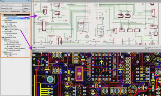
With the components in mind, the design process moves to the schematic capture stage.
This involves creating a detailed diagram that represents the electrical connections between the components. Utilizing specialized software tools, such as Eagle, Altium Designer, or KiCad, can greatly facilitate this process. These tools offer a range of features that help in accurately capturing the schematic, ensuring that all connections are logically sound and that the design adheres to best practices in circuit design.
Transitioning from the schematic to the layout design is the next critical step.
This involves arranging the physical placement of components on the PCB and routing the electrical connections between them. The layout design must consider factors such as signal integrity, thermal management, and electromagnetic compatibility. Proper placement and routing are essential to minimize interference and ensure reliable operation of the circuit. Additionally, attention must be paid to the board’s dimensions and layer count, as these will impact both the cost and manufacturability of the PCB.
As the layout design progresses, it is important to perform design rule checks (DRC) to identify any potential issues that could affect the functionality or manufacturability of the PCB.
These checks help ensure that the design complies with the manufacturing capabilities and constraints of the chosen PCB fabrication service. Once the design passes these checks, it is advisable to simulate the circuit to verify its performance under various conditions. Simulation tools can provide valuable insights into how the circuit will behave in real-world scenarios, allowing for adjustments to be made before proceeding to fabrication.
After finalizing the design, the next step is to generate the necessary files for manufacturing.
These typically include Gerber files, which contain the information needed to produce each layer of the PCB, as well as a bill of materials (BOM) that lists all the components required for assembly. It is crucial to review these files thoroughly to ensure accuracy and completeness, as any errors at this stage can lead to costly delays or rework.
Finally, selecting a reputable PCB manufacturer is essential to ensure the quality and reliability of the finished product.
Factors to consider when choosing a manufacturer include their experience, capabilities, lead times, and customer support. Once the manufacturer is selected, the design files are submitted for production, and the anticipation of receiving the custom PCB begins.
In conclusion, designing a custom printed circuit board is a complex but rewarding process that demands attention to detail and a methodical approach. By following these steps and leveraging the right tools and resources, you can successfully create a PCB that meets the specific needs of your project, paving the way for innovation and technological advancement.
The Future Of Custom Printed Circuit Board Manufacturing
The future of custom printed circuit board (PCB) manufacturing is poised for significant transformation, driven by technological advancements and evolving industry demands. As the backbone of modern electronic devices, PCBs are integral to the functionality and efficiency of a wide array of products, from consumer electronics to industrial machinery. The increasing complexity and miniaturization of electronic components necessitate innovative approaches in PCB manufacturing, prompting a shift towards more customized solutions.
One of the most notable trends in the future of custom PCB manufacturing is the integration of advanced materials and fabrication techniques.
Traditional PCBs, typically made from fiberglass and copper, are being supplemented with materials like flexible polymers and ceramics. These materials offer enhanced performance characteristics, such as improved thermal management and mechanical flexibility, which are crucial for applications in wearable technology and high-frequency communication devices. Moreover, the adoption of additive manufacturing, or 3D printing, is revolutionizing the way PCBs are designed and produced. This technology allows for rapid prototyping and the creation of complex, multi-layered circuits that were previously difficult to achieve with conventional methods.
In addition to material innovations, the future of custom PCB manufacturing is being shaped by the increasing use of automation and artificial intelligence (AI).
Automation streamlines the production process, reducing human error and increasing efficiency. AI, on the other hand, is being leveraged to optimize PCB design and layout, ensuring that circuits are not only functional but also cost-effective and reliable. Machine learning algorithms can analyze vast amounts of data to predict potential design flaws and suggest improvements, significantly reducing the time and resources required for testing and iteration.
Furthermore, the demand for environmentally sustainable manufacturing practices is influencing the future of custom PCB production.
As electronic waste becomes a growing concern, manufacturers are exploring eco-friendly materials and processes. For instance, the use of biodegradable substrates and lead-free soldering techniques is gaining traction. Additionally, recycling and reusing PCB components are becoming more prevalent, driven by both regulatory requirements and consumer expectations for sustainable products.
The globalization of the electronics industry also plays a crucial role in shaping the future of custom PCB manufacturing.
As companies seek to reduce costs and improve supply chain efficiency, there is a growing trend towards outsourcing PCB production to regions with lower labor costs. However, this globalization is balanced by the need for localized manufacturing capabilities, particularly for industries that require rapid turnaround times and high levels of customization. As a result, we are likely to see a hybrid approach, where certain aspects of PCB production are centralized while others are tailored to meet local demands.
In conclusion, the future of custom printed circuit board manufacturing is characterized by a confluence of technological advancements, automation, sustainability, and globalization.
These factors are driving the industry towards more efficient, flexible, and environmentally conscious production methods. As the demand for sophisticated electronic devices continues to grow, the ability to produce highly customized PCBs will be essential for manufacturers seeking to maintain a competitive edge. By embracing these emerging trends, the PCB industry is well-positioned to meet the challenges and opportunities of the future, ensuring that it remains a vital component of the global electronics landscape.
Common Mistakes To Avoid When Creating Custom Printed Circuit Boards
Creating custom printed circuit boards (PCBs) is a complex process that requires meticulous attention to detail and a thorough understanding of both design and manufacturing principles. As the backbone of modern electronic devices, PCBs must be designed with precision to ensure functionality and reliability. However, even experienced designers can fall prey to common mistakes that can compromise the performance of the final product. By being aware of these pitfalls, one can significantly enhance the quality and efficiency of the PCB design process.
One of the most frequent errors in PCB design is inadequate planning.
Before diving into the design phase, it is crucial to have a comprehensive understanding of the project requirements, including the electrical, mechanical, and thermal constraints. Failing to establish clear objectives can lead to design iterations that are both time-consuming and costly. Therefore, it is advisable to create a detailed schematic and layout plan that considers all aspects of the project from the outset.
Another common mistake is neglecting to adhere to design rules and guidelines.
Each PCB manufacturer has specific design rules that must be followed to ensure manufacturability. These rules often pertain to trace widths, spacing, and layer stack-ups. Ignoring these guidelines can result in boards that are difficult or impossible to manufacture, leading to delays and increased costs. To avoid this, designers should familiarize themselves with the manufacturer’s capabilities and limitations early in the design process.
Moreover, improper component placement can severely impact the performance of a PCB.
Components should be strategically placed to minimize signal interference and ensure efficient heat dissipation. Placing components too close together can lead to crosstalk and other signal integrity issues, while poor thermal management can cause overheating and reduce the lifespan of the board. To mitigate these risks, designers should use simulation tools to analyze the thermal and electrical performance of their layouts before finalizing the design.
Transitioning to another critical aspect, the importance of thorough testing and validation cannot be overstated.
Skipping or rushing through the testing phase is a mistake that can have dire consequences. Prototyping and testing allow designers to identify and rectify potential issues before mass production. This step is essential for verifying that the PCB meets all functional requirements and operates as intended under various conditions. By investing time in rigorous testing, designers can avoid costly rework and ensure a high-quality end product.
Furthermore, overlooking the importance of documentation is a mistake that can lead to confusion and errors during the manufacturing process.
Comprehensive documentation, including detailed schematics, assembly drawings, and a bill of materials, is essential for ensuring that the manufacturer accurately produces the PCB. Clear and precise documentation facilitates communication between the designer and manufacturer, reducing the likelihood of misunderstandings and mistakes.
In conclusion, while designing custom printed circuit boards is a challenging endeavor, being mindful of common mistakes can greatly enhance the success of the project. By prioritizing thorough planning, adhering to design rules, optimizing component placement, conducting rigorous testing, and maintaining clear documentation, designers can create PCBs that meet their intended specifications and perform reliably. As technology continues to advance, the demand for high-quality PCBs will only increase, making it imperative for designers to refine their skills and avoid these common pitfalls.