Design and Implementation of a Humidity Sensor PCB
Abstract
Humidity sensors are essential components in various applications, including environmental monitoring, industrial automation, and consumer electronics. The design of a printed circuit board (PCB) for a humidity sensor requires careful consideration of signal integrity, power management, and sensor interfacing. This article discusses the key aspects of designing a humidity sensor PCB, including schematic design, layout considerations, material selection, and testing procedures. A step-by-step guide is provided to help engineers and hobbyists develop an efficient and reliable humidity sensing system.
1. Introduction
Humidity sensors measure the amount of water vapor in the air, providing critical data for climate control, medical devices, and agricultural systems. The performance of these sensors depends heavily on the PCB design, which must ensure accurate signal acquisition and minimal noise interference. This article explores the PCB design process for a capacitive humidity sensor, one of the most commonly used types due to its high accuracy and stability.

2. Humidity Sensor Working Principle
Capacitive humidity sensors consist of a hygroscopic dielectric material sandwiched between two electrodes. As humidity changes, the dielectric absorbs or releases water vapor, altering the capacitance. This change is converted into an electrical signal, which is then processed by a microcontroller.
Key Components in a Humidity Sensor Circuit
- Humidity Sensor IC (e.g., HDC1080, SHT31)
- Microcontroller (e.g., Arduino, ESP32, STM32)
- Power Supply Circuit (LDO Regulator)
- Signal Conditioning Circuit (Amplifiers, Filters)
- Communication Interface (I2C, SPI, UART)
3. Schematic Design
The schematic diagram defines the electrical connections between components. Below is a breakdown of essential sections:
3.1 Sensor Interface
Most digital humidity sensors (e.g., HDC1080) use I2C communication. The schematic should include:
- Proper pull-up resistors (typically 4.7kΩ) for SDA and SCL lines.
- Decoupling capacitors (0.1µF) near the sensor’s VDD pin.
3.2 Power Supply
A stable power supply is crucial for sensor accuracy. A low-dropout (LDO) regulator (e.g., AMS1117-3.3V) is recommended.
- Input capacitor (10µF) for noise filtering.
- Output capacitor (1µF) for stability.
3.3 Microcontroller Connection
The microcontroller reads sensor data via I2C/SPI. Ensure proper level shifting if using different voltage domains (e.g., 5V MCU with 3.3V sensor).
4. PCB Layout Considerations
A well-designed PCB layout minimizes noise and ensures signal integrity. Key considerations include:
4.1 Component Placement
- Place the humidity sensor away from heat sources (e.g., voltage regulators).
- Keep analog and digital sections separated to reduce interference.
4.2 Grounding and Power Planes
- Use a solid ground plane to minimize noise.
- Separate analog and digital grounds, connected at a single point.
- Route power traces with sufficient width to avoid voltage drops.
4.3 Signal Routing
- Keep I2C/SPI traces short and parallel to reduce crosstalk.
- Avoid running high-speed signals near analog sensor lines.
4.4 Environmental Protection
- If the sensor is exposed to harsh environments, consider conformal coating or a protective enclosure.
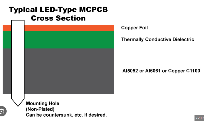
5. Material Selection
- PCB Substrate: FR-4 is common, but high-frequency applications may require Rogers material.
- Trace Width: Follow IPC standards for current-carrying capacity.
- Surface Finish: ENIG (Electroless Nickel Immersion Gold) for better corrosion resistance.
6. Testing and Calibration
After fabrication, the PCB must be tested:
- Continuity Test: Check for short circuits or open traces.
- Power Test: Verify stable voltage levels.
- Sensor Communication Test: Use an oscilloscope to check I2C signals.
- Calibration: Compare readings with a reference hygrometer and adjust firmware if necessary.
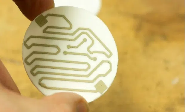
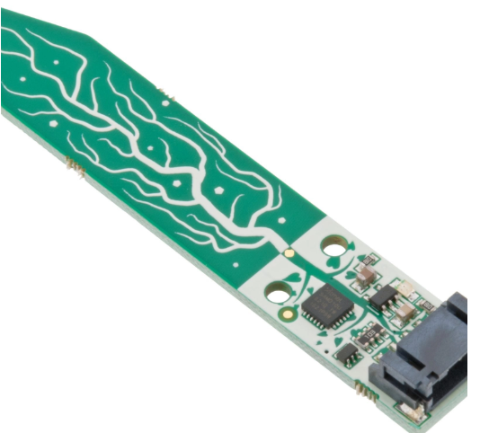
7. Example PCB Design (HDC1080-Based Humidity Sensor)
Below is a simplified PCB design approach:
Schematic
- HDC1080 (I2C Interface)
- STM32F103 (Microcontroller)
- 3.3V LDO Regulator
- Pull-up Resistors (4.7kΩ on SDA/SCL)
- Decoupling Capacitors (0.1µF)
PCB Layout
- 2-Layer Design (Top Layer: Signals, Bottom Layer: Ground Plane)
- Sensor Placement: Near the edge for better air exposure.
- Minimal Trace Lengths for I2C lines.
8. Conclusion
Designing a humidity sensor PCB involves careful schematic design, optimal component placement, and noise reduction techniques. By following best practices in layout and material selection, engineers can develop reliable and accurate humidity sensing systems. Future improvements may include wireless connectivity (Bluetooth/Wi-Fi) for IoT applications.