Design for Manufacturability (DFM) in PCB Production: Key Principles and Best Practices
Introduction
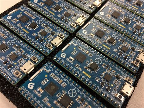
Printed Circuit Boards (PCBs) are the backbone of modern electronics, enabling the functionality of devices ranging from smartphones to industrial machinery. However, designing a PCB that works in theory is not enough—it must also be manufacturable at scale with high reliability and yield. This is where Design for Manufacturability (DFM) comes into play.
DFM is a systematic approach to optimizing PCB designs for efficient, cost-effective, and defect-free manufacturing. By incorporating DFM principles early in the design phase, engineers can avoid costly rework, reduce production delays, and improve product quality. This article explores the key aspects of PCB DFM, including design rules, material selection, fabrication considerations, assembly constraints, and testing strategies.
1. Understanding PCB DFM
DFM for PCBs involves designing boards in a way that aligns with manufacturing capabilities while minimizing potential defects. The primary goals of DFM include:
- Reducing production costs by minimizing material waste and rework.
- Improving yield by avoiding design-related manufacturing failures.
- Enhancing reliability by ensuring robust electrical and mechanical performance.
- Shortening time-to-market by preventing late-stage design changes.
Key Stakeholders in DFM
- Design Engineers – Must understand manufacturing constraints.
- PCB Fabricators – Provide design rules based on their equipment.
- Assembly Houses – Ensure components can be placed and soldered correctly.
- Test Engineers – Verify that the PCB can be tested efficiently.
2. PCB Fabrication DFM Considerations
A. Material Selection
Choosing the right PCB materials is crucial for manufacturability and performance:
- FR-4 – The most common substrate, suitable for most applications.
- High-Frequency Materials (e.g., Rogers, Teflon) – Needed for RF/microwave circuits.
- Flex & Rigid-Flex Materials – Used in space-constrained or bendable applications.
- Copper Weight – Thicker copper improves current handling but complicates etching.
B. Layer Stackup Design
A well-planned stackup ensures signal integrity and manufacturability:
- Symmetrical Layer Arrangement – Prevents warping during lamination.
- Controlled Impedance Layers – Critical for high-speed designs.
- Proper Dielectric Thickness – Avoids impedance mismatches.
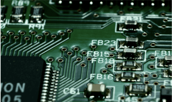
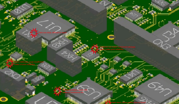
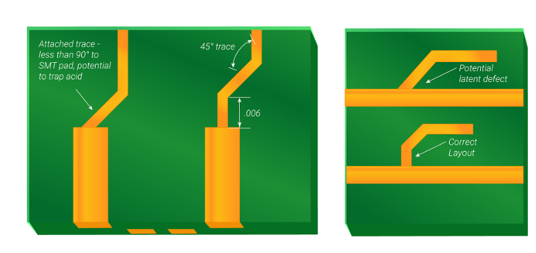
C. Trace and Space Requirements
- Minimum Trace Width/Spacing – Must comply with the fabricator’s capabilities (e.g., 3/3 mil for advanced PCBs).
- Avoid Acute Angles – Can lead to acid traps during etching.
- Teardrops at Pads – Strengthens connections and reduces breakout risks.
D. Via Design
- Through-Hole Vias – Standard but consume more space.
- Blind/Buried Vias – Used in HDI designs but increase cost.
- Microvias – Essential for high-density interconnects (HDI).
- Via-in-Pad – Helps with miniaturization but requires careful soldering.
E. Copper Balancing
Uneven copper distribution can cause warping:
- Use Thieving Pads – Small copper fills to balance etching.
- Avoid Large Copper Pour Areas – Can lead to thermal imbalances.
F. Solder Mask and Silkscreen
- Solder Mask Clearance – Prevents solder bridging.
- Silkscreen Legibility – Ensures component labels are readable.
- Avoid Silkscreen Over Pads – Can interfere with soldering.
3. PCB Assembly DFM Considerations
A. Component Placement
- Minimum Spacing Between Components – Prevents soldering issues.
- Orientation Consistency – Helps automated assembly.
- Thermal Management – High-power components need proper heat dissipation.
B. Land Pattern Design
- IPC-7351 Standards – Ensure proper pad sizes for components.
- Avoid Tombstoning – Balanced pad sizes for passive components.
- Solder Paste Mask – Must align with stencil design.
C. Soldering Considerations
- Surface Finish Selection (HASL, ENIG, OSP, Immersion Silver) – Affects solderability.
- Reflow Profile Compatibility – Components must withstand reflow temperatures.
- Mixed Technology (SMT + THT) – Requires careful process planning.
D. Panelization
- Breakaway Tabs or V-Scoring – Facilitates depanelization.
- Fiducial Marks – Aid in pick-and-place alignment.
- Avoid Components Near Panel Edges – Prevents damage during depaneling.
4. Testing and Inspection DFM
A. Design for Test (DFT)
- Test Points Accessibility – Ensures probes can reach critical nodes.
- Boundary Scan (JTAG) – Simplifies testing of complex boards.
- In-Circuit Test (ICT) Compatibility – Requires test pad placement.
B. Automated Optical Inspection (AOI)
- Clear Contrast Between Pads and Substrate – Helps defect detection.
- Avoid Shadowing – Tall components shouldn’t block inspection.
C. Functional Testing
- Test Fixture Design – Must align with board layout.
- Power and Ground Test Points – Essential for validation.

5. Common DFM Pitfalls and How to Avoid Them
- Ignoring Fabricator Guidelines – Always consult the manufacturer’s capabilities.
- Overly Complex Designs – Simplifying where possible reduces failure risks.
- Inadequate Thermal Relief – Can lead to soldering defects.
- Poor Documentation – Ensure Gerber files, drill files, and assembly drawings are accurate.
6. DFM Software and Tools
Several tools help enforce DFM rules:
- Valor NPI (Siemens) – Advanced DFM analysis.
- Cadence DFM Checker – Integrates with Allegro.
- Altium Designer DFM – Built-in manufacturability checks.
- Mentor Xpedition – Provides real-time DFM feedback.
Conclusion
Designing PCBs with DFM in mind is essential for cost-effective, high-yield manufacturing. By following best practices in fabrication, assembly, and testing, engineers can avoid costly redesigns and production delays. Collaboration between design teams and manufacturers is key to ensuring that a PCB not only functions as intended but can also be reliably mass-produced.
As PCB technology evolves with trends like HDI, flexible circuits, and advanced materials, DFM will remain a critical factor in successful electronics manufacturing. Investing time in DFM early in the design process pays off in reduced costs, faster production, and higher-quality end products.
By adhering to industry standards, leveraging DFM software, and maintaining clear communication with fabrication and assembly partners, engineers can achieve optimal manufacturability without compromising performance.