Design for Manufacturing and Assembly in PCB Design: Key Considerations for Optimal Production
Introduction
Printed Circuit Board (PCB) design is a critical phase in electronics development, bridging the conceptual and physical realization of a product. However, a well-functioning schematic does not always translate into a manufacturable and assemblable PCB. To ensure cost-effective, reliable, and high-quality production, designers must incorporate Design for Manufacturing (DFM) and Design for Assembly (DFA) principles early in the design process.
This article explores the key aspects of PCB design that influence manufacturability and assemblability, covering design rules, material selection, component placement, soldering considerations, and testing strategies.
1. Understanding DFM and DFA in PCB Design
1.1 Design for Manufacturing (DFM)
DFM focuses on optimizing the PCB layout to minimize fabrication issues, reduce costs, and improve yield. Key DFM considerations include:
- Trace Width and Spacing: Adhering to manufacturer capabilities to avoid shorts or open circuits.
- Drill Hole Sizes and Pad Design: Ensuring proper annular rings to prevent drill breakout.
- Copper Balancing: Avoiding warpage by distributing copper evenly across layers.
- Material Selection: Choosing substrates that meet thermal, mechanical, and electrical requirements.
1.2 Design for Assembly (DFA)
DFA ensures that the PCB can be efficiently and accurately assembled with minimal defects. Important DFA factors include:
- Component Placement: Minimizing placement errors and ensuring accessibility for automated assembly.
- Soldering Compatibility: Selecting appropriate pad geometries for reflow or wave soldering.
- Component Orientation: Standardizing component alignment to reduce assembly errors.
- Testability: Incorporating test points for in-circuit testing (ICT) and functional validation.
2. Key PCB Design Considerations for Manufacturability
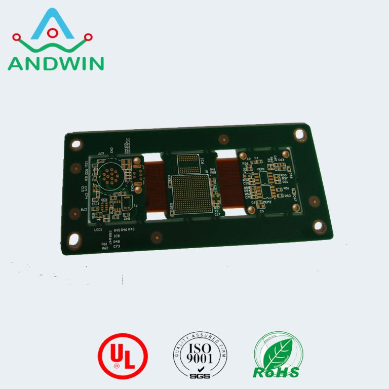
2.1 Layer Stackup and Material Selection
The layer stackup must align with the fabrication capabilities of the PCB manufacturer. Considerations include:
- Dielectric Thickness: Ensuring impedance control for high-speed signals.
- Copper Weight: Balancing current-carrying capacity with etching precision.
- Material Properties: FR-4 is common, but high-frequency designs may require Rogers or polyimide materials.
2.2 Trace and Space Requirements
- Minimum Trace Width/Spacing: Must comply with the manufacturer’s process capabilities (e.g., 4/4 mil for standard PCBs, tighter for HDI).
- Impedance Control: Critical for high-speed designs; requires precise dielectric spacing and trace geometry.
2.3 Via Design and Placement
- Through-Hole vs. Microvias: Through-hole vias are cost-effective, while microvias enable high-density interconnects (HDI).
- Via-in-Pad: Useful for dense designs but requires filling and plating to prevent solder wicking.
- Annular Ring Requirements: Sufficient copper around drilled holes to ensure reliability.
2.4 Solder Mask and Silkscreen
- Solder Mask Clearance: Prevents bridging between pads while ensuring proper solder adhesion.
- Silkscreen Legibility: Component designators and polarity markings must be clear for assembly and debugging.
3. PCB Design for Efficient Assembly (DFA)
3.1 Component Placement Strategies
- Pick-and-Place Optimization: Components should be arranged to minimize robotic arm movement.
- Orientation Consistency: Polarized components (diodes, capacitors) should follow a uniform direction.
- Clearance for Reflow Soldering: Sufficient spacing between components to prevent shadowing and tombstoning.
3.2 Footprint and Pad Design
- Land Pattern Compliance: Following IPC-7351 standards to ensure proper solder joint formation.
- Thermal Relief Pads: Used for through-hole components to prevent excessive heat dissipation during soldering.
3.3 Soldering Process Considerations
- Reflow vs. Wave Soldering: Surface-mount devices (SMDs) use reflow, while through-hole components may require wave soldering.
- Mixed Technology Boards: Requires careful planning to accommodate both soldering methods.
3.4 Testability and Debugging Features
- Test Points: Include accessible test pads for automated testing.
- Boundary Scan (JTAG): Facilitates testing of complex digital circuits.
- Functional Test Fixtures: Design should allow for bed-of-nails or flying probe testing.
4. Common DFM/DFA Pitfalls and How to Avoid Them
4.1 Insufficient Design Rule Checks (DRC)
- Solution: Use automated DRC tools to validate spacing, annular rings, and manufacturability constraints.
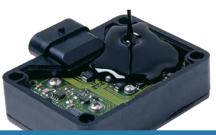
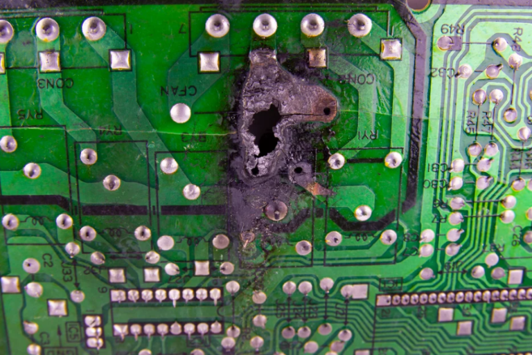
4.2 Poor Thermal Management
- Solution: Incorporate thermal vias, proper copper pours, and heatsinks where necessary.
4.3 Inadequate Documentation
- Solution: Provide a comprehensive fabrication and assembly drawing, including layer stackup, drill table, and assembly notes.
4.4 Overlooking Panelization Requirements
- Solution: Design with panelization in mind, including breakaway tabs and fiducial markers for alignment.
5. The Role of Collaboration Between Designers and Manufacturers
Close communication with PCB fabricators and assembly houses is crucial. Key steps include:
- Early Engagement: Consult manufacturers during the design phase to avoid costly revisions.
- Prototyping and Feedback: Test prototypes to identify and resolve DFM/DFA issues before mass production.
- Design for Cost (DFC): Balance performance requirements with cost-effective manufacturing choices.
6. Future Trends in PCB DFM/DFA
- Advanced Materials: Growth in flexible and high-frequency PCB materials.
- Automated DFM Tools: AI-driven design analysis for real-time manufacturability feedback.
- Miniaturization: Increasing demand for HDI and embedded component technologies.

Conclusion
Designing PCBs with manufacturability and assemblability in mind is essential for reducing production costs, improving yield, and ensuring product reliability. By integrating DFM and DFA principles—such as proper material selection, optimized component placement, and thorough testing strategies—engineers can streamline the transition from design to production. Collaboration with manufacturers, adherence to industry standards, and leveraging advanced design tools will further enhance PCB quality and performance in an increasingly complex electronics landscape.
By prioritizing DFM/DFA, companies can achieve faster time-to-market, higher product reliability, and greater cost efficiency in PCB production.