Designing and Building a Custom Intervalometer PCB for Time-Lapse Photography
Introduction
Time-lapse photography is a fascinating technique that captures a series of images at set intervals and combines them into a video, creating the illusion of time moving quickly. To achieve this, photographers rely on an intervalometer, a device that triggers the camera shutter at predefined intervals. While commercial intervalometers are widely available, building a custom Printed Circuit Board (PCB) for an intervalometer can be a rewarding DIY project for electronics and photography enthusiasts.
In this article, we will explore the process of designing and assembling a custom intervalometer PCB, covering the following aspects:
- Understanding the Basics of an Intervalometer
- Circuit Design and Component Selection
- PCB Layout and Fabrication
- Assembly and Testing
- Software and Calibration
By the end, you will have a functional, programmable intervalometer that can be used with DSLR or mirrorless cameras.
1. Understanding the Basics of an Intervalometer
An intervalometer is essentially a programmable timer that sends a trigger signal to a camera at specified intervals. Most modern cameras have built-in interval shooting modes, but a standalone intervalometer offers more flexibility, especially for long-duration time-lapses.
Key Features of an Intervalometer
- Adjustable delay (time before the first shot)
- Adjustable interval (time between shots)
- Exposure duration control (for bulb mode)
- Total shot count or duration limit
- External trigger compatibility (for remote shutter release)
For our custom PCB, we will design a microcontroller-based intervalometer with these features.
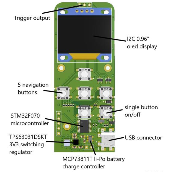
2. Circuit Design and Component Selection
The core of our intervalometer will be a microcontroller (MCU), which will handle timing and trigger signals. We’ll also need supporting components such as resistors, capacitors, a display, and input buttons.
Main Components
- Microcontroller (ATmega328P or STM32): Handles timing and logic.
- OLED/LCD Display: Shows settings like interval, delay, and shot count.
- Buttons/Switches: For user input (adjusting intervals, starting/stopping).
- Optocoupler or Relay: Isolates the camera trigger circuit to avoid electrical interference.
- Power Supply (Battery + Voltage Regulator): Typically 3.7V LiPo or 9V battery with a 3.3V/5V regulator.
Schematic Design
Using a PCB design tool like KiCad or EasyEDA, we create a schematic with:
- MCU and its supporting circuitry (crystal oscillator, decoupling capacitors).
- User interface (buttons, rotary encoder, display).
- Camera trigger circuit (optocoupler for safe triggering).
- Power management (voltage regulator, battery connector).
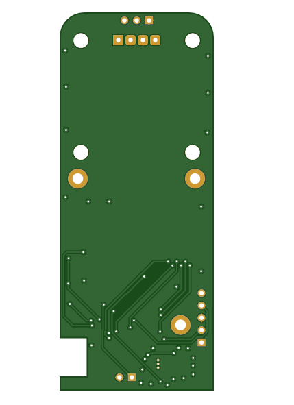
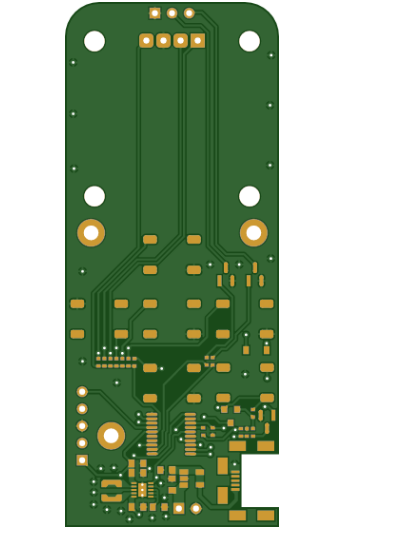
3. PCB Layout and Fabrication
Once the schematic is complete, we move to PCB layout, where components are physically placed and routed.
Key Considerations
- Component Placement: Group related components (e.g., MCU near its oscillator).
- Power Traces: Ensure sufficient width for current flow.
- Signal Integrity: Avoid long parallel traces to reduce noise.
- Mechanical Constraints: Fit inside an enclosure, with buttons and display accessible.
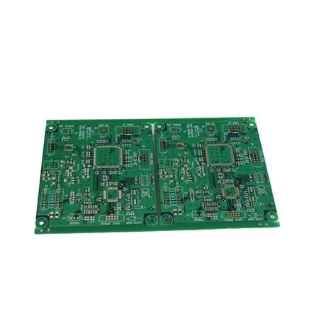
PCB Fabrication
After finalizing the design, we export Gerber files and send them to a PCB manufacturer (e.g., JLCPCB, PCBWay). Typical specs:
- 2-layer board (cheap and sufficient for this project).
- FR-4 material (standard for most PCBs).
- Silkscreen and solder mask for readability and protection.
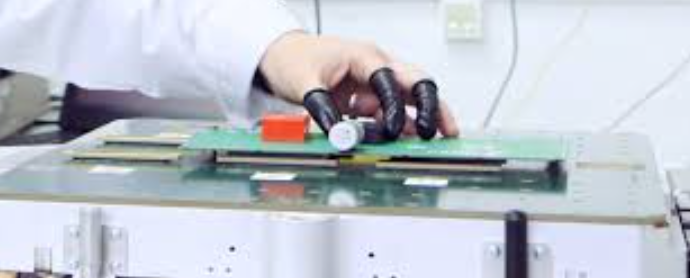
4. Assembly and Testing
Once the PCB arrives, we proceed with assembly and testing.
Soldering Components
- Start with smallest components (resistors, capacitors).
- Move to larger components (MCU, connectors).
- Use a multimeter to check for shorts or incorrect connections.
Testing the Circuit
- Power Test: Verify voltage levels (3.3V/5V) at the regulator output.
- MCU Programming: Flash firmware using an ISP programmer or USB-to-Serial adapter.
- Display and Buttons: Check if the UI responds correctly.
- Camera Trigger Test: Connect to a camera and verify triggering.

5. Software and Calibration
The firmware (written in C/C++ or Arduino) controls the intervalometer’s logic.
Key Functions
- Timer Interrupts: For precise timing.
- User Input Handling: Adjust intervals via buttons.
- Display Updates: Show current settings.
- Trigger Signal Generation: Send a pulse to the camera.
Example Arduino Code Snippet
#include <Wire.h>
#include <LiquidCrystal_I2C.h>

LiquidCrystal_I2C lcd(0x27, 16, 2); // LCD setup
const int shutterPin = 8; // Camera trigger pin
unsigned long interval = 5000; // Default interval: 5 seconds

void setup() {
  pinMode(shutterPin, OUTPUT);
  lcd.init();
  lcd.backlight();
  lcd.print("Intervalometer");
}

void loop() {
  digitalWrite(shutterPin, HIGH); // Trigger camera
  delay(100); // Mimic shutter press
  digitalWrite(shutterPin, LOW);

  lcd.setCursor(0, 1);
  lcd.print("Next shot in: ");
  lcd.print(interval / 1000);
  lcd.print("s");

  delay(interval); // Wait for next shot
}
Calibration
- Adjust timing delays if the camera doesn’t trigger correctly.
- Optimize power consumption for battery life.
Conclusion
Building a custom intervalometer PCB is an excellent project for photographers and electronics hobbyists. It provides full control over time-lapse settings while offering a deeper understanding of PCB design, microcontroller programming, and circuit assembly.
With this guide, you can design, fabricate, and assemble your own intervalometer, tailored to your specific needs. Future enhancements could include Bluetooth/Wi-Fi control, light sensors, or motion triggers for advanced functionality.
Would you like additional details on any specific part of the process? Happy building!