Electromagnetic interference and anti-interference problems in PCB multilayer boards.
Electromagnetic compatibility (EMC) is an emerging comprehensive discipline that mainly studies electromagnetic interference and anti-interference problems. Electromagnetic compatibility means that electronic equipment or systems do not reduce performance indicators due to electromagnetic interference under the specified electromagnetic environment level, and the electromagnetic radiation generated by them is not greater than the specified limit level, does not affect the normal operation of other systems, and achieves the purpose of non-interference and reliable operation between equipment and equipment, and between systems.
Electromagnetic interference (EMI) is caused by the electromagnetic interference source transferring energy to the sensitive system through the coupling path.
It includes three basic forms: conduction by wires and common ground wires, radiation through space, or near-field coupling. Practice has proved that even if the circuit schematic is designed correctly, improper design of the printed circuit board will have an adverse effect on the reliability of electronic equipment. Therefore, ensuring the electromagnetic compatibility of the printed circuit board is the key to the design of the entire system. This article mainly discusses electromagnetic compatibility technology and its application in the design of multilayer printed circuit boards (PCBs).
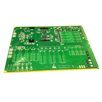
PCB is the support for circuit elements and devices in electronic products. It provides electrical connections between circuit elements and devices and is the most basic component of various electronic devices. Nowadays, large-scale and ultra-large-scale integrated circuits have been widely used in electronic devices, and the installation density of components on printed circuit boards is getting higher and higher, and the signal transmission speed is getting faster and faster. The EMC problems caused by this are becoming more and more prominent. PCB is divided into single-sided board (single-layer board), double-sided board (double-layer board) and multi-layer board. Single-sided board and double-sided board are generally used for circuits with low and medium density wiring and circuits with low integration. Multi-layer boards use high-density wiring and high-integration circuits. From the perspective of electromagnetic compatibility, single-sided board and double-sided board are not suitable for high-speed circuits. Single-sided and double-sided wiring can no longer meet the requirements of high-performance circuits. The development of multi-layer wiring circuits provides a possibility to solve the above problems, and its application is becoming more and more extensive.
In the EMC design considerations of PCB, the first thing involved is the setting of layers; the number of layers of a single board is composed of the number of power supply, ground layers and signal layers; in the EMC design of products, in addition to the selection of components and circuit design, good PCB design is also a very important factor.
The key to PCB EMC design is to minimize the return area as much as possible and let the return path flow in the direction we designed. The design of the layer is the basis of the PCB. How to do a good job in the PCB layer design to optimize the EMC effect of the PCB?

1.Design ideas for PCB layers
The core of PCB stacking EMC planning and design ideas is to reasonably plan the signal return path and minimize the return area of the signal from the single board mirror layer as much as possible, so that the magnetic flux is canceled or minimized.
2.Single board mirror layer
The mirror layer is a complete copper-clad plane layer (power layer, ground layer) adjacent to the signal layer inside the PCB. It mainly has the following functions:
Reduce return noise: The mirror layer can provide a low-impedance path for the signal layer return, especially when there is a large current flowing in the power distribution system, the role of the mirror layer is more obvious.
Reduce EMI: The existence of the mirror layer reduces the area of the closed loop formed by the signal and the return flow, reducing EMI;
Reduce crosstalk: It helps to control the crosstalk problem between signal lines in high-speed digital circuits. By changing the height of the signal line from the mirror layer, the crosstalk between the signal lines can be controlled. The smaller the height, the smaller the crosstalk;
Impedance control to prevent signal reflection.
(2)Selection of mirror layer
Both the power supply and ground planes can be used as reference planes, and have a certain shielding effect on the internal wiring;
Relatively speaking, the power plane has a higher characteristic impedance, and there is a large potential difference with the reference level. At the same time, the high-frequency interference on the power plane is relatively large;
From the perspective of shielding, the ground plane is generally grounded and used as a reference point for the reference level. Its shielding effect is far better than that of the power plane;
When selecting a reference plane, the ground plane should be preferred, and the power plane should be second.
2.Principle of flux cancellation
According to Maxwell’s equations, all electrical and magnetic effects between discrete charged bodies or currents are transmitted through the intermediate area between them, regardless of whether the intermediate area is a vacuum or a solid substance. In PCB, magnetic flux always propagates in the transmission line. If the RF return path is parallel to its corresponding signal path, the magnetic flux on the return path is in opposite directions to the magnetic flux on the signal path. At this time, they are superimposed on each other, and the effect of flux cancellation is obtained.
3.The essence of magnetic flux cancellation
The essence of magnetic flux cancellation is actually the control of the signal return path. The specific schematic diagram is as follows:
4.How to use the right-hand rule to explain the magnetic flux cancellation effect when the signal layer is adjacent to the ground layer?
The explanation is as follows:
When a current flows through the wire, a magnetic field will be generated around the wire, and the direction of the magnetic field is determined by the right-hand rule.
When there are two wires close to each other and parallel, as shown in the figure below, the current of one conductor flows outward and the current of the other conductor flows inward. If the currents flowing through the two wires are the signal current and its return current, respectively, then the two currents are equal in magnitude and opposite in direction, so their magnetic fields are also equal in magnitude and opposite in direction, so they can cancel each other out.
Specific principles for PCB layer design:
(1) There should be a complete ground plane (shielding) under the component surface and welding surface;
(2) Try to avoid two signal layers being directly adjacent to each other;
(3) All signal layers should be adjacent to the ground plane as much as possible;
(4) Key signal wiring layers such as high frequency, high speed, and clock should have an adjacent ground plane