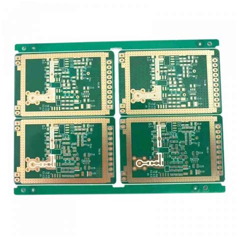
Elimination Technology of PCB Silver Layer – Full Text
1.Current Status
As we all know, since printed circuit boards cannot be reworked after assembly, the cost loss caused by scrapping due to micro voids is the highest. Although eight of the PWB manufacturers noticed this defect due to customer rejections, this type of defect was mainly reported by the assembly manufacturers. Solderability issues were not reported by PWB manufacturers at all, and only three assembly manufacturers mistakenly attributed the “tin shrinkage” problem (which means that the solder only fills half the hole depth after wave soldering) on high aspect ratio (HAR) thick boards with large heat sinks/surfaces inside to the silver layer. After more in-depth research and verification by the original equipment manufacturer (OEM) on this issue, it was found that this problem was entirely due to solderability issues caused by the circuit board design and had nothing to do with the silver process or other final surface treatment methods.

2.Root Cause Analysis
Through the root cause analysis of the defects, these defect rates can be minimized through a combination of process improvement and parameter optimization. The Galvani effect usually appears under the cracks between the solder mask and the copper surface. During the silver deposition process, because the gap of the crack is very small, the silver ion supply to this place is limited by the silver deposition liquid, but the copper here can be corroded into copper ions, and then the silver deposition reaction occurs on the copper surface outside the crack. Because ion conversion is the driving force of the silver deposition reaction, the degree of attack on the copper surface under the crack is directly related to the thickness of the silver deposition. 2Ag++1Cu=2Ag+1Cu++ (+ is a metal ion that loses an electron) Any of the following reasons will form cracks: excessive side etching/development or poor bonding between the solder mask and the copper surface; uneven electroplated copper layer (thin copper at the hole mouth); obvious deep scratches on the copper substrate under the solder mask.
Corrosion is caused by the reaction of sulfur or oxygen in the air with the metal surface. The reaction of silver and sulfur will form a yellow silver sulfide (Ag2S) film on the surface. If the sulfur content is high, the silver sulfide film will eventually turn black. There are several ways for silver to be contaminated by sulfur, air (as mentioned above) or other pollution sources, such as PWB packaging paper. The reaction of silver with oxygen is another process. Usually, oxygen reacts with copper under the silver layer to produce dark brown cuprous oxide. This defect is usually caused by the very fast silver deposition speed, forming a low-density silver deposition layer, which makes the copper at the bottom of the silver layer easy to contact with the air, so the copper will react with the oxygen in the air. The loose crystal structure has larger intergranular gaps, so a thicker silver deposition layer is required to achieve oxidation resistance. This means that a thicker silver layer must be deposited in production, which increases production costs and increases the probability of solderability problems, such as microvoids and poor soldering.
Copper exposure is usually related to the chemical process before silver deposition. This defect appears after the silver deposition process, mainly because the residual film that was not completely removed by the previous process hinders the deposition of the silver layer. The most common is the residual film caused by the solder mask process, which is caused by the incomplete development in the developer, that is, the so-called “residual film”, which hinders the silver deposition reaction. The mechanical treatment process is also one of the reasons for copper exposure. The surface structure of the circuit board will affect the uniformity of the contact between the board surface and the solution. Insufficient or excessive solution circulation will also form an uneven silver layer.
Ionic contamination The ionic substances on the surface of the circuit board will interfere with the electrical properties of the circuit board. These ions mainly come from the silver solution itself (remaining in the silver layer or under the solder mask). Different silver solutions have different ion contents. The higher the ion content of the solution, the higher the ion contamination value under the same water washing conditions. The porosity of the silver layer is also one of the important factors affecting ion contamination. The silver layer with high porosity is easy to retain ions in the solution, making water washing more difficult, and eventually leading to a corresponding increase in the ion contamination value. The post-washing effect will also directly affect the ion contamination. Insufficient water washing or unqualified water quality will cause ion contamination to exceed the standard.
Microvoids are usually less than 1 mil in diameter. The voids above the metal interface compound between the solder and the welding surface are called microvoids. Because it is actually a “planar cavitation group” on the welding surface, it greatly reduces the welding bonding force. OSP, ENIG and immersion silver will have microvoids on the surface. The root cause of their formation has not yet been determined, but several influencing factors have been confirmed. Although all microvoids in the immersion silver layer occur on the surface of thick silver (thickness greater than 15μm), not all thick silver layers will have microvoids. Microvoids are more likely to occur when the copper surface structure at the bottom of the immersion silver layer is very rough. The occurrence of microvoids also seems to be related to the type and composition of organic matter co-deposited in the silver layer. In response to the above-mentioned phenomenon, original equipment manufacturers (OEMs), equipment manufacturing service providers (EMS), PWB manufacturers and chemical suppliers have conducted several welding studies under simulated conditions, but none of them can completely eliminate microvoids.
3.Preventive measures
The formulation of preventive measures needs to consider the contribution of chemicals and equipment to various defects in actual production in order to avoid or eliminate defects and improve yield. The prevention of the Galvani effect can be traced back to the copper plating process of the previous process. For high aspect ratio holes and micro-vias, uniform electroplating layer thickness helps to eliminate the hidden dangers of the Galvani effect. Excessive corrosion or side etching during the film stripping, etching and tin stripping processes will promote the formation of cracks, and micro-etching solution or other solutions will remain in the cracks. Despite this, the problem of solder mask is still the main cause of the Galvani effect. Most defective boards with the Galvani effect have side etching or solder mask peeling, which mainly comes from the exposure and development process. Therefore, if the solder mask is “positive foot” after development and the solder mask is completely cured, the Galvani effect problem can be almost eliminated. To obtain a good silver layer, the silver position must be 100% metal copper, each tank solution has good through-hole ability, and the solution in the through-hole can be effectively exchanged. If it is a very fine structure, such as an HDI board, it is very useful to install ultrasonic or ejector in the pre-treatment and silver bath solution. For the production management of the silver process, controlling the micro-etching rate to form a smooth, semi-bright surface can also improve the Galvani effect. For original equipment manufacturers (OEMs), designs in which large copper surfaces or high aspect ratio through-holes are connected to fine lines should be avoided as much as possible to eliminate the hidden dangers of the Galvani effect. For chemical suppliers, the silver immersion solution should not be very aggressive, and the appropriate pH value should be maintained. The silver immersion speed should be controlled and the expected crystal structure should be generated, so that the best corrosion resistance can be achieved with the thinnest silver thickness.
Corrosion can be reduced by increasing the density of the coating and reducing the porosity. Use sulfur-free materials for packaging, and seal to isolate the board from the air, which also prevents the sulfur entrained in the air from contacting the silver surface. It is best to store the packaged boards in an environment with a temperature of 30°C and a relative humidity of 40%. Although the shelf life of silver immersion boards is very long, the first-in-first-out principle should still be followed during storage.
Copper exposure can be reduced or eliminated by optimizing the pre-silver immersion process. To achieve this goal, the copper surface can be checked by “water breaking” test or “bright spot” test after micro-etching. The clean copper surface can maintain the water film for at least 40 seconds. Regularly maintain the equipment to ensure that the solution circulation is uniform and stable, and optimize the time, temperature, and stirring through DOE to obtain the best silver immersion operation parameters, thereby ensuring the ideal thickness and high-quality silver layer. Ultrasonic waves or jets are used as needed to improve the wetting ability of the silver solution for micro-vias, high aspect ratio holes and thick boards. It also provides a feasible solution for the production of HDI boards. These auxiliary mechanical methods can be applied in pre-treatment and silver solution to ensure that the hole wall is completely wetted.
Ionic contamination can be reduced by reducing the ion concentration of the silver solution. For this reason, the ion content of the silver solution should be kept as low as possible without affecting the performance of the solution. Usually the final cleaning section is cleaned with deionized water for at least 1 minute, and the ion content (anions and cations) must be regularly tested to see if it meets industrial standards. The results of these tests must be recorded and retained to distinguish the main sources of contamination.
Microvoids are the most difficult defect to prevent because the real cause of their occurrence is not yet clear. As mentioned earlier, we already know that some factors seem to cause microvoids or accompany microvoids, and these factors can be eliminated or minimized to control the occurrence of microvoids. Among them, the thickness of the silver layer is the most significant factor in causing microvoids, so controlling the thickness of the silver layer is the first step. Secondly, the micro-etching speed and silver deposition speed should be adjusted to obtain a smooth and uniform surface structure. The purity of the silver deposition layer at different time points during the service life of the test bath should also be tested to monitor the organic content in the silver deposition layer. The reasonable silver content should be controlled above 90% (atomic ratio).
4.Ideal process-AlphaSTAR
In addition to excellent performance, an “ideal process” must also meet the safety, environmental protection and reliability requirements of the electronics industry announced on July 1, 2006.
Although Lesi Chemical has the patent rights for the AlphaLEVEL product series as early as 1994, Lesi Chemical has continued to improve and develop the process, and has successfully developed the third generation of silver deposition technology for printed circuit boards-AlphaSTAR. The AlphaSTAR process is specially designed to meet today’s increasingly stringent final surface treatment requirements. It solves the above-mentioned problems that lead to scrapping of circuit boards, increased costs, environmental protection and safety, and complies with relevant regulations that may affect the printed circuit board industry now and in the future. This process has a total of 7 steps (three of which are water washing steps), and its performance and advantages are described as follows:
Pretreatment is divided into the following four steps: degreasing, water washing, micro etching and water washing. The surface tension of the degreasing solution is very low and can wet all copper surfaces, which not only eliminates the problem of exposed copper, but also promotes the deposition of the silver layer in high aspect ratio holes and micro-vias. The unique micro etching formula can produce a micro-roughened, semi-bright surface structure, which is conducive to the formation of a silver layer with a fine and dense crystal structure. Therefore, even when the thickness of the silver layer is very low, a high-density, low-porosity silver layer can be obtained. This greatly improves the corrosion resistance of the silver layer.
Silver immersion is divided into the following three steps: pre-immersion, silver immersion and the final deionized water washing. There are three purposes for setting up pre-immersion. One is to use it as a sacrificial solution to prevent copper and other substances from being brought into the micro etching tank to contaminate the silver immersion solution. The second is to provide a clean copper surface for the silver immersion replacement reaction, so that the copper surface obtains the same chemical environment and pH value as in the silver immersion solution. Since the composition of the pre-dip is the same as that of the silver immersion solution (except for metallic silver), the third function of this process is to automatically replenish the silver immersion tank. The only thing consumed in the silver immersion reaction is metallic silver. The change in the content of organic components in the silver immersion solution is only the loss caused by the carry-out of the tank solution. The pre-dip and silver immersion solution have the same composition. The amount brought in by the pre-dip is equal to the amount brought out by the silver immersion, so the silver immersion solution will not accumulate unnecessary organic matter. The silver immersion reaction is carried out by the replacement reaction between copper and silver ions. The copper surface treated with AlphaSTAR micro-etching solution can ensure that a uniform and consistent silver immersion layer can be slowly generated at a controlled silver immersion speed. The slow silver immersion speed is conducive to the deposition of a dense crystal structure, avoiding the growth of particles caused by precipitation and agglomeration, and forming a high-density silver layer. This compact, moderately thick (6-12u”) silver layer not only has high corrosion resistance, but also has very good conductivity. The silver immersion solution is very stable, has a long service life, and is insensitive to light and trace halides. Other advantages of AlphaSTAR include: greatly shortened downtime, low ion contamination and low equipment cost.
5. Conclusion
The AlphaSTAR process combines the best performance of several final surface treatments. It meets and exceeds the global printed circuit board industry’s requirements for solderability, reliability, safety and regulatory compliance. The AlphaSTAR process has a wide operating window; it is easy to operate, control and maintain, can be reworked, and has the lowest production cost among similar final surface treatments. The AlphaSTAR process eliminates or reduces the direct impact of the six issues related to the silver immersion process discussed above on high-quality products. In addition, this process complies with RoHS and WEEE regulations, and the silver immersion layer is completely lead-free.


