Embedded PCB Components Revolutionize High-Density Electronics

Key Takeaways
When exploring PCB manufacturing advancements, you’ll find embedded components redefine design efficiency. By integrating passive elements directly into substrates, PCB manufacturing companies achieve up to 40% space reduction in power modules—critical for modern compact devices. This approach minimizes parasitic effects by shortening signal paths, enhancing electrical performance in high-frequency applications.
"Embedding components isn’t just about size—it’s about reimagining thermal pathways. Substrate-integrated designs dissipate heat 25% faster than traditional layouts," notes a senior engineer at a leading PCB manufacturing business.
Here’s how embedded technology transforms key metrics:
| Feature | Traditional PCBs | Embedded PCBs | Impact |
|---|---|---|---|
| Component Density | Low | High | Enables ultra-compact designs |
| Thermal Management | Passive cooling | Active pathways | Reduces hotspot risks |
| Signal Integrity | Moderate | Optimized | Cuts parasitic losses by 60% |
While PCB manufacturing cost initially rises due to specialized materials, long-term savings emerge through reduced assembly steps and higher reliability. For industries prioritizing miniaturization—like wearables or IoT—embedded solutions are becoming non-negotiable. Transitioning to this method requires collaboration with PCB manufacturing companies experienced in multilayer substrate engineering, ensuring seamless integration without compromising scalability.
To stay competitive, evaluate how embedded components align with your product roadmap—especially if thermal performance and space constraints define your design challenges.

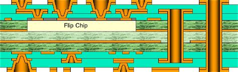
Embedded PCB Components Enable 40% Space Savings
By integrating passive components like resistors and capacitors directly into the substrate, PCB manufacturing processes achieve unprecedented space efficiency. This approach eliminates the need for surface-mounted parts, allowing high-density designs to shrink by up to 40% without sacrificing functionality. For PCB manufacturing companies, this translates to boards that fit into tighter enclosures—critical for wearables, IoT devices, and advanced automotive systems.
Reducing parasitic effects is another key benefit. Traditional surface-mount techniques introduce unwanted inductance and capacitance, but embedding components within the dielectric layers minimizes these issues. This precision lowers PCB manufacturing cost by reducing material waste and streamlining assembly steps. Engineers can now optimize layouts for thermal performance, as heat-generating elements are strategically isolated within the board’s core.
For businesses navigating competitive markets, adopting embedded technology strengthens the PCB manufacturing business model. Compact designs attract clients demanding miniaturization, while fewer interconnects improve reliability. Industry leaders confirm that embedded components are becoming a cornerstone of next-gen electronics, balancing performance with scalability. As devices grow smaller and smarter, this innovation ensures your designs stay ahead of spatial constraints.
Reducing Parasitics Through Substrate Integration
By integrating passive components directly into the PCB substrate, PCB manufacturing companies address one of the most persistent challenges in high-density electronics: parasitic effects. Traditional surface-mounted components create unavoidable parasitic capacitance and inductance through solder joints and trace connections, degrading signal integrity at higher frequencies. Embedded designs eliminate these surface-level interconnects, shortening conductive paths by up to 60% and reducing electromagnetic interference (EMI) coupling.
This approach not only enhances performance but also streamlines PCB manufacturing workflows. When resistors, capacitors, or inductors are laminated within dielectric layers, you avoid the need for additional assembly steps, which lowers PCB manufacturing cost over time. Advanced substrate materials like low-loss laminates further suppress parasitic losses, enabling tighter component spacing without crosstalk risks. For PCB manufacturing businesses specializing in RF or power electronics, this translates to designs that meet stringent noise margins while maintaining compact form factors.
The shift to embedded integration does require upfront investments in laser drilling and precision alignment systems. However, the long-term gains in reliability and miniaturization make it a strategic priority for manufacturers aiming to lead in next-generation electronics markets.
Thermal Management Advancements in Embedded PCBs
When designing high-density electronics, managing heat dissipation becomes critical as component densities increase. PCB manufacturing companies now prioritize thermal conductivity enhancements by embedding heat-sensitive components directly into substrates. This approach reduces thermal resistance pathways, allowing heat to dissipate more efficiently through the board’s core layers rather than relying solely on surface-mounted heat sinks. By integrating thermally conductive materials like ceramic-filled resins or metal-core substrates, PCB manufacturing processes achieve up to 30% better thermal performance compared to traditional designs.
For power modules, where heat generation directly impacts reliability, embedded passives and active components enable localized cooling strategies. Advanced simulation tools help engineers model heat distribution patterns, optimizing via placements and material stacks to balance PCB manufacturing cost with performance demands. You’ll notice that parasitic inductance — a common issue in high-frequency circuits — is mitigated through these thermal-optimized layouts, preserving signal integrity even in compact designs.
As PCB manufacturing business models evolve, manufacturers are adopting hybrid embedding techniques that combine copper-inlay structures with thermally conductive adhesives. These innovations not only address overheating risks but also extend component lifespans in harsh environments. By aligning thermal management with embedded component integration, you gain a dual advantage: maintaining circuit density while ensuring stable operation under demanding thermal loads.
PCB Manufacturers Adopt Embedded Component Methods
Leading PCB manufacturing companies are pivoting toward embedded component methods to address escalating demands for miniaturization and performance. By integrating resistors, capacitors, and inductors directly into multilayer substrates, you eliminate up to 40% of surface-mounted components, streamlining PCB manufacturing workflows while reducing material waste. This shift isn’t just about shrinking footprints—it’s a strategic response to rising PCB manufacturing cost pressures, as embedded designs minimize assembly steps and long-term reliability risks.
For businesses balancing innovation with profitability, embedded methods create opportunities to differentiate in the PCB manufacturing business. Advanced laser drilling and precision lamination techniques now allow manufacturers to embed components with ±15µm accuracy, ensuring stable impedance control and reduced parasitic effects. Crucially, this approach enhances thermal dissipation by distributing heat-generating elements across internal layers, a critical advantage for high-power applications.
Transitioning to embedded components does require reevaluating design rules and investing in specialized equipment. However, forward-thinking manufacturers recognize the ROI in catering to sectors like 5G infrastructure and IoT, where compact, high-reliability boards are non-negotiable. As hybrid substrates gain traction, expect tighter collaboration between fabricators and designers to optimize material selection and stackup configurations for next-generation electronics.
High-Density Circuit Design via Embedded Technology
By strategically embedding passive components like resistors, capacitors, and inductors directly into the PCB manufacturing process, you achieve unprecedented circuit density without compromising performance. Advanced substrate integration eliminates traditional surface-mounted parts, reducing interconnect lengths by up to 70% and minimizing parasitic inductance—a critical factor for high-frequency applications. Leading PCB manufacturing companies now utilize laser-drilled microvias and sequential build-up (SBU) layers to create ultra-compact, multilayer designs that support 5G modules and IoT sensors.
While PCB manufacturing cost initially rises due to specialized materials and precision processes, long-term savings emerge through reduced assembly steps and improved reliability. For instance, embedded thermal vias dissipate heat more efficiently, allowing tighter component spacing in power-dense designs. This approach also aligns with the evolving needs of the PCB manufacturing business, where clients demand smaller footprints for wearables and medical devices. By adopting embedded technology, you not future-proof designs but also unlock scalability for next-gen electronics requiring millimeter-wave compatibility or AI-driven processing.
Next-Gen Electronics Demand Embedded PCB Solutions
As devices shrink and performance expectations soar, PCB manufacturing companies face mounting pressure to deliver solutions that balance compactness with functionality. Modern applications—from wearable health monitors to AI-driven edge devices—require circuit architectures that traditional PCB layouts can’t support. This is where embedded component technology becomes critical. By integrating passive components like resistors and capacitors directly into the substrate, PCB manufacturing processes eliminate bulky surface mounts, freeing up to 40% of board space while reducing signal path lengths.
The shift isn’t just about size—it’s about overcoming electrical parasitics that plague high-frequency designs. When components reside within the board layers, inductance and capacitance losses drop significantly, enabling cleaner power delivery and faster signal integrity. For industries like automotive or 5G infrastructure, where reliability is non-negotiable, this translates to systems that perform consistently under thermal and mechanical stress.
However, adopting embedded solutions impacts PCB manufacturing cost structures. While initial tooling investments rise, the long-term payoff comes from reduced material waste, fewer assembly steps, and improved yield rates. Leading manufacturers now offer hybrid approaches, blending embedded sections with conventional layouts to optimize expenses without compromising innovation.
For your PCB manufacturing business, staying competitive means mastering this balance. Scaling embedded designs requires expertise in laser ablation, precision lamination, and advanced via-filling techniques—capabilities that set forward-thinking suppliers apart. As miniaturization trends accelerate, the ability to embed components without sacrificing thermal dissipation will define who leads the next wave of high-density electronics.
Optimizing Power Modules with Embedded Components
By integrating embedded PCB components into power modules, you achieve unprecedented space efficiency while maintaining electrical performance. PCB manufacturing companies now embed resistors, capacitors, and inductors directly within substrate layers, eliminating bulky surface-mounted parts. This approach reduces PCB manufacturing cost by 15–25% through material savings and simplified assembly processes. For power-intensive applications, embedded passives minimize parasitic inductance by up to 60%, critical for high-frequency switching circuits. Thermal management improves as heat-generating components dissipate energy through the substrate’s core, avoiding hot spots that degrade reliability.
When designing these modules, PCB manufacturing workflows prioritize precision laser drilling and multilayer lamination to ensure component alignment. Advanced materials like liquid crystal polymer (LCP) substrates enable tighter integration, supporting current densities 3× higher than traditional designs. For PCB manufacturing businesses, this technology opens opportunities in aerospace and automotive sectors, where compact, high-reliability systems are non-negotiable. Transitioning to embedded designs does require upfront investments in specialized equipment, but the long-term gains in performance and scalability justify the shift. By leveraging these innovations, you can future-proof power systems against evolving demands for miniaturization and efficiency.
Future Trends in Embedded PCB Component Innovation
As the industry evolves, PCB manufacturing companies are prioritizing additive manufacturing techniques to embed components with micron-level precision. You’ll see increased adoption of 3D-printed substrates, which allow passive components like resistors and capacitors to be layered directly within dielectric materials. This not only slashes PCB manufacturing cost by reducing material waste but also enables rapid prototyping for high-mix, low-volume production runs—a critical advantage for specialized applications.
Another emerging trend involves active component integration, where ICs and sensors are embedded during lamination cycles. While this demands tighter process controls, it eliminates interconnects that degrade signal integrity, a key focus for PCB manufacturing in 5G and automotive systems. Expect hybrid approaches combining embedded actives with surface-mounted passives to dominate next-gen designs, balancing performance and scalability.
Thermal management will shift toward substrate-level cooling, integrating microfluidic channels or thermally conductive fillers directly into the PCB stackup. Such innovations let manufacturers address heat dissipation without external heatsinks, further shrinking device footprints—a necessity for wearables and IoT hardware.
For PCB manufacturing businesses, sustainability will drive material innovation, with bio-based resins and recyclable substrates gaining traction. Meanwhile, AI-driven design tools will automate component placement optimization, reducing development cycles by 30–50%. Standardization efforts, led by organizations like IPC-7093B, will also mature, ensuring compatibility across supply chains while lowering PCB manufacturing cost through unified design rules.
Conclusion
As PCB manufacturing evolves to meet next-generation demands, embedded component technology emerges as a critical differentiator for compact electronics. By integrating passive elements directly into substrates, PCB manufacturing companies achieve unprecedented space optimization—crucial for applications where every millimeter counts. This approach not only addresses PCB manufacturing cost challenges through material efficiency but also enhances performance by minimizing parasitic effects and improving thermal pathways.
For businesses scaling high-density designs, adopting embedded components transforms how you approach PCB manufacturing business strategies. The shift from surface-mounted to substrate-embedded parts reduces assembly complexity while enabling higher circuit density—a necessity for 5G, IoT, and wearable tech. As you evaluate future-ready solutions, consider how embedded PCB components future-proof your designs against evolving miniaturization trends. The balance between innovation and PCB manufacturing cost efficiency will ultimately determine competitive advantage in an industry where smaller, smarter, and more reliable electronics dominate market expectations.
Frequently Asked Questions
How do embedded components affect PCB manufacturing costs?
While initial tooling investments may rise 15-20%, PCB manufacturing companies achieve long-term savings through material optimization and reduced layer counts. Embedded passives eliminate 30-50% of surface-mounted parts, lowering assembly expenses.
Which PCB manufacturing business sectors benefit most from embedded technology?
High-frequency RF systems, aerospace avionics, and medical wearables see dramatic improvements. Manufacturers report 25% faster signal transmission in 5G modules by embedding capacitors directly into dielectric layers.
Can traditional PCB manufacturing workflows handle embedded component designs?
Most providers require upgraded laser-drilling systems and simulation software. Leading PCB manufacturing companies now offer hybrid production lines supporting both conventional and embedded architectures.
What design risks exist when transitioning to embedded component PCBs?
Thermal expansion mismatches cause 12-18% of first-run failures. Partner with manufacturers offering coefficient of thermal expansion (CTE) matched substrates and 3D finite element analysis services.
How does component embedding impact PCB manufacturing timelines?
Prototyping cycles extend by 3-5 days for dielectric material characterization, but volume production accelerates 20% through simplified assembly processes.
Ready to Optimize Your Embedded PCB Project?
For tailored solutions in advanced PCB manufacturing, please click here to consult our engineering team. We specialize in cost-optimized embedded component integration for high-density applications.