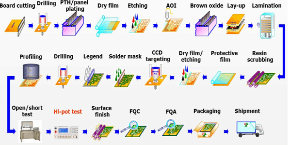
Equipment involved in pcb manufacturing
Essential Tools for PCB Prototyping
Printed Circuit Board (PCB) prototyping is a critical phase in the development of electronic devices, serving as the bridge between conceptual design and mass production. The process involves a series of steps that require precision and accuracy, necessitating the use of specialized equipment. Understanding the essential tools involved in PCB prototyping is crucial for ensuring the quality and functionality of the final product.
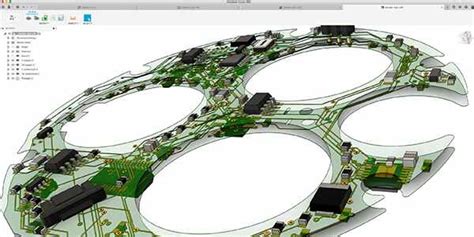
To begin with, the design phase of PCB prototyping relies heavily on Computer-Aided Design (CAD) software.
This software allows engineers to create detailed schematics and layout designs, ensuring that all components are correctly placed and connected. CAD software is indispensable for visualizing the circuit and making necessary adjustments before moving on to the physical prototyping stage.
Once the design is finalized, the next step involves transferring the design onto a physical substrate.
This is where a photoplotter comes into play. A photoplotter is used to create a photomask, which is essentially a high-resolution image of the PCB layout. This photomask is then used in the photolithography process to transfer the design onto a copper-clad board. The precision of the photoplotter is vital for ensuring that the intricate details of the PCB design are accurately reproduced.
Following the creation of the photomask, the next essential tool is the etching machine.
The etching process involves removing unwanted copper from the board, leaving behind only the desired circuit pattern. This is typically achieved using a chemical solution that dissolves the excess copper. The etching machine must be carefully calibrated to ensure that the etching process is uniform and does not damage the remaining copper traces.
After etching, the board undergoes a drilling process to create holes for component leads and vias.
A CNC drilling machine is commonly used for this purpose. This machine is capable of drilling precise holes at specified locations, which is crucial for the proper placement and soldering of components. The accuracy of the CNC drilling machine ensures that the holes are correctly aligned with the circuit design, preventing potential connectivity issues.
Once the holes are drilled, the next step is to apply a solder mask to the board.
A solder mask is a protective layer that prevents solder bridges from forming between closely spaced solder pads. This is typically done using a solder mask applicator, which evenly coats the board with the solder mask material. The application of the solder mask is essential for preventing short circuits and ensuring the reliability of the PCB.
Following the application of the solder mask, the board is ready for component placement and soldering.
A pick-and-place machine is used to accurately position components on the board. This machine uses a combination of vacuum and mechanical arms to pick up components from a reel or tray and place them onto the board with high precision. The pick-and-place machine is essential for handling small and delicate components, ensuring that they are correctly positioned for soldering.
Finally, the soldering process is carried out using a reflow oven or a wave soldering machine, depending on the type of components and soldering method used. The reflow oven is used for surface-mount components, where solder paste is applied to the pads before the components are placed. The board is then heated in the reflow oven, causing the solder paste to melt and form a solid connection. For through-hole components, a wave soldering machine is used, where the board is passed over a wave of molten solder, creating secure connections.
In conclusion, PCB prototyping involves a series of precise and intricate steps, each requiring specialized equipment. From CAD software and photoplotters to etching machines, CNC drilling machines, solder mask applicators, pick-and-place machines, and soldering equipment, each tool plays a vital role in ensuring the accuracy and functionality of the final PCB. Understanding the importance of these tools is essential for anyone involved in the field of PCB manufacturing.
Advanced Soldering Equipment for PCB Assembly
In the realm of printed circuit board (PCB) manufacturing, advanced soldering equipment plays a pivotal role in ensuring the reliability and functionality of the final product. As the complexity of electronic devices continues to escalate, the demand for precision and efficiency in PCB assembly has never been higher. Consequently, the industry has seen significant advancements in soldering technology, which are essential for meeting these rigorous standards.
One of the most critical pieces of equipment in advanced PCB soldering is the reflow oven.
Reflow soldering is a process where solder paste, which has been applied to the PCB, is melted to create electrical connections between components and the board. Modern reflow ovens are equipped with multiple heating zones, allowing for precise temperature control throughout the soldering process. This precision is crucial for preventing defects such as solder bridges or cold joints, which can compromise the integrity of the PCB. Additionally, these ovens often feature advanced monitoring systems that ensure consistent thermal profiles, further enhancing the reliability of the soldering process.
Transitioning from reflow ovens, another indispensable tool in advanced PCB soldering is the wave soldering machine.
Wave soldering is typically used for through-hole components, which are inserted into pre-drilled holes on the PCB. The machine generates a wave of molten solder that flows over the bottom of the board, soldering the component leads to the PCB. Modern wave soldering machines are designed with sophisticated fluxing systems and preheating stages, which help to improve solder joint quality and reduce the risk of thermal shock to the components. Moreover, these machines often incorporate automated conveyor systems, which enhance throughput and ensure consistent results.
In addition to reflow and wave soldering, selective soldering machines have become increasingly prevalent in advanced PCB assembly.
Selective soldering is used for applications where only specific areas of the PCB require soldering, making it ideal for mixed-technology boards that combine surface-mount and through-hole components. These machines utilize precise nozzles to apply solder only to the designated areas, minimizing the risk of thermal damage to sensitive components. Furthermore, selective soldering machines are often equipped with advanced software that allows for the programming of complex soldering patterns, thereby increasing flexibility and efficiency in the manufacturing process.
Another critical aspect of advanced soldering equipment is the use of automated optical inspection (AOI) systems.
AOI systems are employed to inspect solder joints and component placement, ensuring that any defects are identified and corrected before the PCB moves to the next stage of production. These systems use high-resolution cameras and sophisticated algorithms to detect issues such as insufficient solder, misaligned components, and solder bridges. By integrating AOI systems into the soldering process, manufacturers can significantly reduce the incidence of defects and improve overall product quality.
Finally, it is essential to consider the role of soldering robots in advanced PCB assembly.
Soldering robots are designed to perform precise soldering tasks with a high degree of accuracy and repeatability. These robots are particularly useful for applications that require fine-pitch soldering or the handling of delicate components. Equipped with advanced vision systems and programmable controllers, soldering robots can adapt to a wide range of PCB designs and soldering requirements, making them a versatile addition to any manufacturing line.
In conclusion, advanced soldering equipment is integral to the success of modern PCB manufacturing. From reflow ovens and wave soldering machines to selective soldering systems, AOI systems, and soldering robots, each piece of equipment plays a crucial role in ensuring the quality and reliability of the final product. As technology continues to evolve, the importance of precision and efficiency in PCB assembly will only grow, underscoring the need for continued innovation in soldering equipment.
Automated Optical Inspection Systems in PCB Manufacturing
Automated Optical Inspection (AOI) systems play a crucial role in the manufacturing of printed circuit boards (PCBs), ensuring the quality and reliability of the final product. These systems are designed to automatically inspect PCBs for defects and inconsistencies, which can be critical in maintaining the high standards required in various industries, including consumer electronics, automotive, aerospace, and medical devices. The integration of AOI systems into the PCB manufacturing process has revolutionized quality control, providing a more efficient and accurate method of inspection compared to traditional manual methods.
To understand the significance of AOI systems, it is essential to recognize the complexity of modern PCBs.
These boards often contain multiple layers, intricate circuitry, and a high density of components, making manual inspection not only time-consuming but also prone to human error. AOI systems address these challenges by utilizing advanced imaging technologies and sophisticated algorithms to detect a wide range of defects, such as soldering issues, component misalignment, and surface contamination. By automating the inspection process, manufacturers can achieve higher throughput and consistency, ultimately leading to improved product quality and reduced production costs.
The operation of AOI systems involves several key components and technologies.
High-resolution cameras capture detailed images of the PCB, which are then analyzed by powerful software algorithms. These algorithms compare the captured images against a predefined set of criteria or a reference model, identifying any deviations that may indicate a defect. The use of multiple lighting techniques, such as bright field, dark field, and 3D imaging, enhances the system’s ability to detect various types of defects. For instance, bright field lighting is effective for identifying surface defects, while dark field lighting is better suited for detecting edge defects and solder joint issues. 3D imaging, on the other hand, provides depth information, allowing for the inspection of component height and coplanarity.
In addition to defect detection, AOI systems offer several other benefits that contribute to the overall efficiency of the PCB manufacturing process.
One such benefit is the ability to provide real-time feedback to the production line. When a defect is detected, the AOI system can immediately alert operators, enabling them to take corrective actions before the defective board progresses further down the production line. This real-time feedback loop helps to minimize the impact of defects on the final product and reduces the likelihood of costly rework or scrap.
Moreover, AOI systems can be integrated with other manufacturing equipment and processes, creating a seamless and automated production environment.
For example, AOI systems can be linked with pick-and-place machines, solder paste inspection (SPI) systems, and reflow ovens, allowing for continuous monitoring and optimization of the entire production process. This integration not only enhances the overall efficiency but also provides valuable data for process improvement and quality assurance.
Furthermore, the data collected by AOI systems can be used for statistical process control (SPC) and trend analysis.
By analyzing defect patterns and trends over time, manufacturers can identify potential issues in the production process and implement preventive measures to address them. This proactive approach to quality control helps to ensure that the manufacturing process remains stable and capable of producing high-quality PCBs consistently.
In conclusion, Automated Optical Inspection systems are indispensable in modern PCB manufacturing, offering a highly efficient and accurate method of quality control. By leveraging advanced imaging technologies and sophisticated algorithms, AOI systems can detect a wide range of defects, provide real-time feedback, and integrate seamlessly with other manufacturing processes. The benefits of AOI systems extend beyond defect detection, contributing to overall process efficiency, data-driven decision-making, and continuous improvement in product quality. As the demand for high-quality PCBs continues to grow, the role of AOI systems in ensuring manufacturing excellence will only become more critical.
The Role of Pick-and-Place Machines in PCB Production
In the intricate world of printed circuit board (PCB) manufacturing, the role of pick-and-place machines is paramount. These sophisticated pieces of equipment are essential for the precise and efficient assembly of electronic components onto PCBs, which are the backbone of virtually all electronic devices. Understanding the function and importance of pick-and-place machines provides insight into the complexities of modern electronics manufacturing.
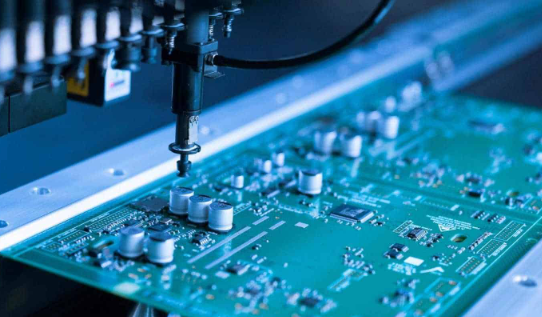
Pick-and-place machines are automated systems designed to place surface-mount devices (SMDs) onto PCBs with high accuracy and speed.
These machines are equipped with advanced vision systems and robotic arms that can handle a wide variety of components, ranging from tiny resistors and capacitors to larger integrated circuits. The process begins with the preparation of the PCB, which is typically coated with a layer of solder paste. This paste acts as an adhesive to hold the components in place before they are permanently soldered.
One of the key advantages of pick-and-place machines is their ability to handle high-volume production runs with remarkable precision.
These machines can place thousands of components per hour, significantly reducing the time and labor required for manual assembly. Moreover, the accuracy of pick-and-place machines ensures that components are placed exactly where they are needed, minimizing the risk of errors that could lead to malfunctioning devices. This level of precision is achieved through the use of sophisticated software algorithms and high-resolution cameras that guide the placement process.
In addition to speed and accuracy, pick-and-place machines offer flexibility in PCB manufacturing.
They can be programmed to handle different types of components and board designs, making them suitable for a wide range of applications. This versatility is particularly important in the electronics industry, where product designs are constantly evolving, and manufacturers need to adapt quickly to new requirements. By using pick-and-place machines, manufacturers can easily switch between different production runs without significant downtime, thereby increasing overall efficiency.
Furthermore, the integration of pick-and-place machines into the broader PCB manufacturing process enhances overall production quality.
These machines work in conjunction with other equipment, such as solder paste printers and reflow ovens, to ensure a seamless assembly process. For instance, after the components are placed on the PCB, the board is typically passed through a reflow oven, where the solder paste is melted to create strong electrical connections. The precise placement of components by the pick-and-place machine ensures that the soldering process is effective, resulting in reliable and high-quality PCBs.
Another important aspect of pick-and-place machines is their role in reducing production costs.
By automating the component placement process, manufacturers can significantly lower labor costs and reduce the likelihood of human error. Additionally, the high throughput of these machines means that more PCBs can be produced in a shorter amount of time, leading to economies of scale. This cost efficiency is crucial in the competitive electronics market, where manufacturers are constantly seeking ways to reduce expenses while maintaining high standards of quality.
In conclusion, pick-and-place machines are indispensable in the PCB manufacturing process. Their ability to place components with high precision and speed, coupled with their flexibility and integration with other manufacturing equipment, makes them a critical asset for electronics manufacturers. By leveraging the capabilities of pick-and-place machines, manufacturers can produce high-quality PCBs efficiently and cost-effectively, meeting the demands of an ever-evolving industry.