Essential Guide to Double Sided PCB Assembly Techniques

Key Takeaways
When exploring double-sided PCB assembly (PCBA), it is essential to grasp a few critical points that ensure the success of your projects. First, understanding the key design considerations for double-sided PCBs can significantly impact the performance and reliability of your circuits. Pay attention to component placement, as optimal layout minimizes signal interference and enhances thermal management.
Moreover, selecting the right manufacturing processes is vital. Different methods can affect the overall quality of assembly; therefore, knowing your options allows for better decision-making that aligns with your project’s needs.
Best practices in component placement and soldering are fundamental in achieving high-quality solder joints, which are crucial for the durability of your PCB assemblies. Prioritize a well-planned soldering strategy that accommodates both manual and automated techniques to maximize efficiency.
Testing and quality assurance processes cannot be overlooked — they play a significant role in identifying issues early, ensuring that every assembled board meets its specifications before deployment.
Lastly, embracing advanced techniques can enhance performance. Techniques such as using specialized materials or incorporating multi-layer designs pave the way for innovative solutions in complex applications.
“A well-designed double-sided PCB is often the backbone of any successful electronic device.”
Introduction to Double-Sided PCB Assembly
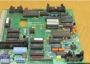
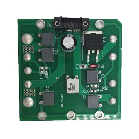
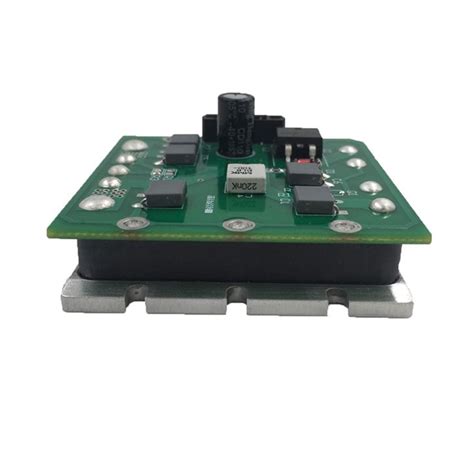
In the realm of electronics, double-sided PCB assembly (often referred to as PCBA) offers significant advantages in terms of design flexibility and functionality. By allowing components to be placed on both sides of the substrate, designers can optimize space and enhance the overall performance of the circuit board. This technique is particularly beneficial for complex circuitry where numerous components are required, as it helps in reducing the footprint while maintaining accessibility for soldering and assembly.
One of the core aspects of double-sided PCB assembly is ensuring proper alignment and registration between layers during manufacturing. Effective design considerations, such as appropriate pad sizes and component placements, are crucial in achieving robust connections while preventing solder bridging—a common issue that negatively impacts circuit reliability.
To visualize this process better, consider the following table, which outlines key elements essential to double-sided PCBA:
| Key Element | Description |
|---|---|
| Layer Alignment | Ensures that both sides align perfectly for optimal performance |
| Component Density | Strategically placing components to maximize space efficiency |
| Solder Mask Management | Proper masking to prevent unwanted solder connections |
| Thermal Relief | Heat dissipation techniques to protect sensitive components |
Moreover, understanding the challenges inherent in double-sided PCB assembly, such as thermal expansion differences between materials or handling during manufacturing, becomes pivotal for achieving a successful end product. Tasks such as soldering require meticulous attention; therefore, familiarity with best practices like using automated placement systems or selective soldering can significantly enhance production efficiency and ensure reliable connections.
In summary, successful double-sided PCB assembly requires a combination of careful design considerations, stringent manufacturing processes, and a focus on best practices throughout production to yield high-quality electronic assemblies that meet performance demands.
Key Design Considerations for Double-Sided PCBs
When embarking on a double-sided PCB assembly (PCBA) project, several crucial design considerations must be kept in mind to ensure optimal functionality and reliability. One of the primary aspects is the layer stack-up, which directly impacts the electrical performance and thermal management of the board. Careful attention to the spacing between traces on each layer can help to minimize crosstalk and signal integrity issues. Additionally, component placement is paramount; components should be arranged to minimize routing complexity, which can significantly enhance manufacturability and reduce costs.
Incorporating via designs effectively facilitates inter-layer connections without overcrowding any single layer with traces. Designers should also prioritize pad sizes and hole tolerances, as these elements are critical to ensuring a successful soldering process during assembly. Furthermore, with advances in technology pushing towards smaller components, designers may need to consider using smaller pads or even placement improvisations like microvias for densely packed areas. The choice of materials plays an essential role as well; selecting high-quality substrates that can withstand thermal fluctuations is vital for maintaining performance during the lifetime of the device. By keeping these considerations in mind, engineers can achieve a well-optimized double-sided PCB that meets both design specifications and enhances overall reliability in their electronic projects.
Manufacturing Processes for Double-Sided PCB Assembly
The manufacturing processes for double-sided PCB assembly (PCBA) encompass several critical steps that ensure optimal performance and reliability. Initially, the process begins with the preparation of the printed circuit board (PCB), which involves cleaning and applying a solder mask to enhance adhesion and prevent solder bridging. Following this, components are typically placed on both sides of the board; this dual-sided approach allows for more efficient use of space and often results in a more compact design.
During the assembly process, techniques such as pick-and-place machines are utilized to accurately position components, ensuring precise alignment for optimal electrical connection. Once components are placed, the next stage is soldering, which can be accomplished through various methods including wave soldering and reflow soldering. Wave soldering is particularly effective for through-hole components on one side, while reflow is used predominantly for surface mount technologies (SMT) on the opposite side.
To achieve reliable connections in double-sided PCBA, both methods may be implemented in conjunction to cater to diverse component types. After soldering, it is essential to perform a thorough inspection; this may include visual checks or automated optical inspection (AOI) systems to identify any defects such as insufficient solder or misaligned components. Ultimately, these manufacturing processes not only facilitate effective pcb assembly but also ensure that the final product adheres to industry standards while meeting customer requirements for quality and functionality.
Best Practices for Component Placement and Soldering
Proper component placement and soldering techniques are essential for successful pcb assembly. In double-sided pcba, the aim is to strategically arrange components to minimize interference and maximize performance. To achieve this, careful consideration should be given to component orientation and accessibility for soldering. Placing larger components closer to the center can help balance weight distribution, while small components should be positioned away from the edges to reduce the likelihood of damage during handling.
When it comes to soldering, using the right techniques can significantly enhance the reliability of your double-sided PCB assembly. Techniques such as wave soldering or reflow soldering vary in effectiveness depending on component type and layout. It’s critical to ensure that solder joints are formed properly; insufficient solder can lead to weak connections, while excessive solder may cause bridging between pads.
Moreover, thermal management is a key factor in the assembly process. Adequate spacing between heat-sensitive components and heat sources prevents damage during soldering. Additionally, it can be beneficial to use a stencil for applying solder paste uniformly across surface mount components, ensuring high-quality joints.
Lastly, adhering to a systematic approach when verifying placements through visual inspection or automated optical inspection (AOI) is highly recommended. By following these best practices in component placement and soldering, you can optimize your pcba projects for enhanced functionality and long-term reliability.
Testing and Quality Assurance in Double-Sided PCB Assembly
To ensure the reliability and performance of double-sided PCB assembly, rigorous testing and quality assurance processes are vital. Effective testing methods include automated optical inspection (AOI), which plays a crucial role in identifying defects on both sides of the PCB before soldering. Furthermore, utilizing functional testing methodologies after assembly confirms that the assembled board operates as intended. It is equally essential to integrate in-circuit testing (ICT) to assess the performance of each component within the circuit, identifying any faults in real time.
Quality assurance in PCBA involves adhering to industry standards such as IPC-A-610, which outlines acceptability requirements for soldered electronics. In this context, assembling teams should be trained not only in the fundamental principles of assembly but also in recognizing and preventing common pitfalls such as poor solder joints or component misalignment. Continuous monitoring of the soldering process, alongside performing stress tests under varying conditions, further bolsters confidence in the reliability and durability of double-sided boards.
Ultimately, an effective quality assurance framework not only reduces manufacturing costs but also enhances customer satisfaction by delivering high-quality pcb assembly products that perform reliably across their intended applications. Implementing these strategic measures leads to a culture of quality excellence within organizations dedicated to double-sided PCB assembly.
Troubleshooting Common Issues in Double-Sided PCBs
When working with double-sided PCB assembly, it’s essential to be aware of some common challenges that may arise during the design and manufacturing process. One prevalent issue is solder bridging, which occurs when excess solder connects two or more pads, potentially shorting the circuit. To address this, careful component placement and adequate solder application are crucial. Another common problem is warping of the PCB during the reflow soldering process, often due to uneven heat distribution. Utilizing proper thermal management techniques can help mitigate this risk.
Additionally, issues such as poor connectivity often manifest as intermittent connections, which can be traced back to inadequate solder joint quality or insufficient cleaning processes before assembly. Ensuring a thorough cleaning procedure before applying solder can greatly enhance the reliability of a pcb assembly. Lastly, discrepancies in dimensions or misalignment between layers can lead to serious functional issues in the final product. Employing meticulous design rules and double-checking alignment during both layout and assembly stages will lower these risks significantly.
By implementing these troubleshooting strategies and consistently applying best practices for pcba, you can optimize performance and reliability in double-sided PCB projects.
Advanced Techniques for Enhanced Performance and Reliability
In the realm of double-sided PCB assembly, leveraging advanced techniques can significantly enhance both performance and reliability of electronic products. One approach is the incorporation of layer stacking to optimize power delivery and signal integrity. By strategically arranging components, designers can minimize signal interference and reduce electromagnetic compatibility issues. Furthermore, the use of via-in-pad technology allows for a more compact layout, facilitating efficient routing of signals while maintaining thermal management. For components that are sensitive to heat, utilizing thermal vias can effectively dissipate excessive heat generated during operation. Additionally, implementing automated optical inspection (AOI) in the manufacturing process ensures that every layer of the PCBA meets strict quality standards. This proactive quality assurance measure minimizes defects and enhances overall circuit performance. Adopting these advanced strategies not only elevates the durability of your designs but also supports consistent production output, ultimately leading to more reliable electronic devices in a competitive market.
Conclusion
In summary, understanding double-sided PCB assembly is crucial for anyone involved in electronics design and manufacturing. As discussed throughout this guide, optimizing pcb assembly techniques can significantly enhance the overall functionality and reliability of electronic products. Incorporating best practices in component placement, soldering, and testing is essential for preventing common issues and ensuring high-quality performance. By leveraging advanced manufacturing processes and adhering to key design considerations, engineers and designers can create robust printed circuit boards that meet the demands of modern technology. Adopting these insights not only streamlines the PCBA production process but also fosters innovation across various applications, from consumer electronics to industrial devices. Ultimately, a well-executed double-sided PCB assembly will help elevate the standard of electronic systems in an increasingly competitive landscape.
FAQs
What is double-sided PCB assembly?
Double-sided PCB assembly refers to the process of placing components on both sides of a printed circuit board (PCB). This technique allows for a more compact design and can accommodate a greater number of components within the same footprint.
What are the main advantages of double-sided PCBs?
The primary advantages include increased component density, improved performance due to shorter signal paths, and enhanced flexibility in design. Using double-sided assembly, engineers can optimize space while maintaining functionality.
How do I decide between single-sided and double-sided PCB assembly?
The choice largely depends on the complexity and functionality required for your project. If your design involves many components or requires high signal integrity, double-sided PCBA is often the preferable choice due to its efficient space utilization and performance capabilities.
What materials are commonly used in double-sided PCB assemblies?
Common materials include FR-4, which is a flame-resistant plastic widely favored for its durability, and aluminum PCBs that provide excellent heat dissipation. The material choice can significantly affect the performance and reliability of the PCB assembly process.
Are there any special considerations for soldering on double-sided PCBs?
Yes, factors such as thermal management, component placement accuracy, and solder paste application require careful attention. Proper techniques are crucial to ensuring that both sides of the board are effectively soldered without causing defects or reducing reliability.