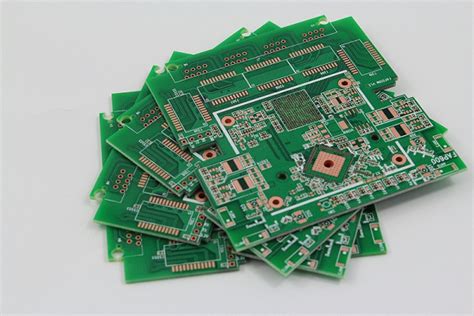
Essential PCB Design and Assembly Techniques
Key Takeaways
Understanding core principles in PCB manufacturing ensures your designs transition smoothly from concept to functional boards. Start by prioritizing design-for-manufacturability (DFM) guidelines—this minimizes errors during fabrication and reduces PCB manufacturing cost. When selecting PCB manufacturing companies, evaluate their expertise in handling your project’s complexity, whether it’s high-density interconnects or mixed-technology assemblies.
Tip: Collaborate with manufacturers early to align design choices with their capabilities, avoiding costly revisions later.
Efficient assembly hinges on balancing surface-mount technology (SMT) and through-hole components based on your application’s mechanical and thermal demands. For PCB manufacturing business scalability, adopt standardized processes like automated optical inspection (AOI) to maintain consistency across batches. Always factor in material selection—using high-Tg substrates or low-loss dielectrics can enhance reliability in demanding environments.
By integrating these strategies, you’ll streamline production timelines, optimize budgets, and deliver robust circuit boards tailored to modern electronics requirements.
PCB Design Fundamentals for Optimal Performance
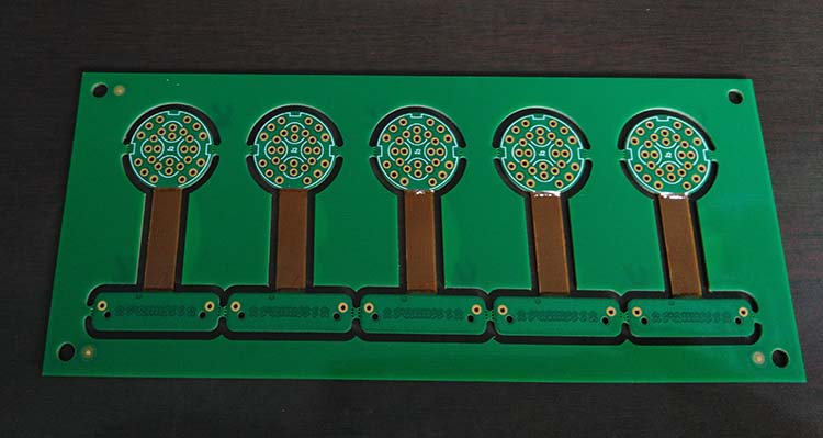
When designing printed circuit boards (PCBs), balancing performance with pcb manufacturing cost requires careful planning. Start by defining clear design rules: trace widths, spacing, and via sizes must align with your chosen pcb manufacturing companies’ capabilities to avoid costly revisions. For example, high-density interconnect (HDI) layouts may boost performance but increase fabrication complexity.
Prioritize component placement to minimize signal interference—group analog and digital sections separately, and ensure power planes are adequately isolated. Proper thermal management techniques, like adding copper pours or heat sinks, prevent overheating in high-power applications. Use design software to simulate electrical behavior, catching errors early and reducing pcb manufacturing business delays.
| Design Choice | Impact on Performance |
|---|---|
| Optimized trace routing | Reduces crosstalk & signal loss |
| Controlled impedance | Ensures high-frequency stability |
| Layer stacking | Balances cost vs. signal integrity |
Collaborating with experienced pcb manufacturing partners early in the design phase helps identify cost-saving opportunities, such as panelization strategies or material alternatives. For instance, selecting FR-4 over ceramic substrates might lower expenses without compromising functionality for most applications. Always reference industry standards like IPC-2221 to validate design decisions. By integrating these principles, you create boards that meet performance targets while staying within budget.
Cost-Effective PCB Fabrication Strategies
To minimize PCB manufacturing cost without compromising quality, start by optimizing your design for material efficiency. Simplify board layouts to reduce unnecessary layers and avoid oversized dimensions, which directly impacts material waste. Collaborate with PCB manufacturing companies early in the design phase to identify areas where standard panel sizes or shared tooling can lower expenses. For instance, using common substrate materials like FR-4 instead of specialized alternatives often balances performance and affordability.
Batch production is another key strategy—consolidating multiple designs into a single fabrication run spreads fixed costs across more units. However, ensure your PCB manufacturing business model accounts for lead time flexibility, as rushing orders typically incurs premium fees. When prototyping, consider "bare-board" testing to catch errors before investing in full assembly.
Advanced techniques like automated routing and Design for Manufacturability (DFM) checks further streamline processes, reducing rework risks. Partnering with manufacturers who offer volume discounts or panelization services can also enhance cost efficiency. Remember, balancing design complexity with production scalability ensures long-term viability in competitive PCB manufacturing markets.
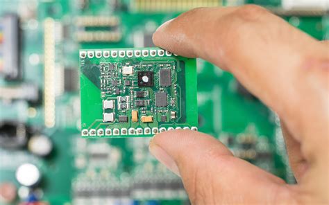
Efficient Assembly Methods for Circuit Boards
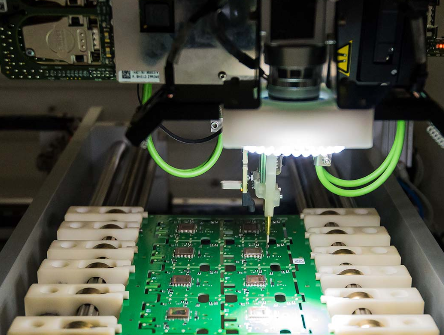
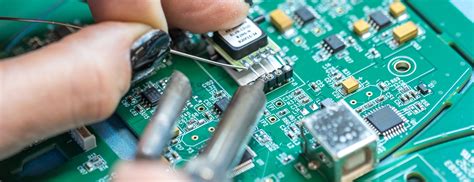
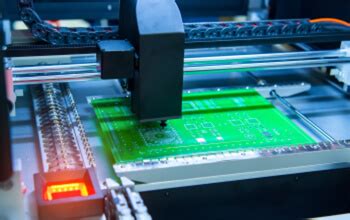
To achieve reliable PCB manufacturing outcomes, refining your assembly process is critical. Start by optimizing component placement using automated pick-and-place machines, which minimize human error while accelerating throughput. Pair this with precision-controlled reflow soldering to ensure consistent joint quality, especially for high-density designs. For PCB manufacturing companies, balancing speed and accuracy directly impacts PCB manufacturing cost—over-engineering can inflate expenses, while under-specifying tools risks defects.
Leverage Design for Manufacturability (DFM) principles early in the process. By collaborating with your PCB manufacturing business partner, you can identify potential assembly bottlenecks, such as inadequate pad spacing or incompatible component sizes. For mixed-technology boards, combining surface-mount and through-hole assembly requires strategic sequencing—mount SMDs first to avoid thermal stress on larger components.
Automated optical inspection (AOI) systems are indispensable for catching misalignments or solder bridges post-assembly. When prototyping, prioritize modular workflows to test assembly feasibility before scaling. This approach not only reduces material waste but also aligns with cost-sensitive PCB manufacturing strategies. Finally, maintain clear documentation for assembly guidelines, ensuring repeatability across batches—a hallmark of professional PCB manufacturing companies.
Troubleshooting Common PCB Manufacturing Errors
When dealing with PCB manufacturing challenges, identifying root causes early saves time and reduces PCB manufacturing cost overruns. Start by inspecting soldering defects—cold joints or bridging often stem from improper temperature profiles during reflow. If traces appear cracked or delaminated, check for thermal stress during assembly or inadequate material selection. For alignment issues, verify that your design files match the fabrication specs, as even minor discrepancies in layer registration can render boards unusable.
Collaborate closely with PCB manufacturing companies to diagnose recurring problems. For example, if via failures persist, they might recommend switching to laser-drilled microvias or adjusting plating thickness. Electrochemical migration—a common cause of short circuits—can often be mitigated through stricter cleanliness protocols or conformal coating.
In high-volume PCB manufacturing business operations, automated optical inspection (AOI) systems help flag defects like missing components or solder voids. However, don’t overlook manual checks for subtle issues like copper weight mismatches or silkscreen inaccuracies. Addressing these systematically ensures reliability while balancing production speed and quality—a critical factor when scaling your output.
Pro tip: Document every troubleshooting step to create a knowledge base, streamlining future problem-solving and fostering continuous improvement in your manufacturing workflow.
Material Selection in Reliable PCB Production
Choosing the right materials is foundational to ensuring PCB manufacturing quality and longevity. Your selection directly impacts thermal stability, signal integrity, and mechanical durability. For instance, FR-4 remains a popular substrate due to its cost-effectiveness and flame resistance, but high-frequency applications may require specialized materials like Rogers laminates to minimize signal loss.
When evaluating PCB manufacturing companies, prioritize those offering material certifications (e.g., UL 94V-0) and compatibility with your design’s electrical and environmental demands. Copper weight and dielectric constant are critical parameters—thicker copper improves current capacity, while lower dielectric constants enhance signal speed.
Balancing PCB manufacturing cost with performance involves strategic trade-offs. Opting for lead-free finishes like ENIG (Electroless Nickel Immersion Gold) might increase upfront expenses but reduces long-term environmental risks. For startups in the PCB manufacturing business, collaborating with suppliers to source bulk materials at negotiated rates can optimize budgets without compromising reliability.
Always consider thermal expansion coefficients—mismatched materials can cause warping or delamination during assembly. By aligning material properties with your application’s requirements, you ensure robust performance across temperature cycles and mechanical stresses.
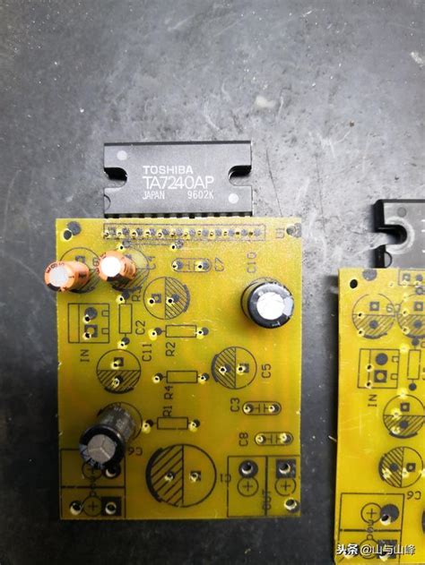
Surface Mount Technology vs Through-Hole Assembly
When choosing between surface mount technology (SMT) and through-hole assembly (THT) for your PCB manufacturing project, understanding their distinct advantages ensures optimal design outcomes. SMT dominates modern electronics due to its compact component placement, enabling higher circuit density and faster automated assembly. This method reduces PCB manufacturing cost by minimizing material waste and labor time—a critical factor for high-volume production runs. However, THT remains relevant for applications requiring mechanical stability, such as connectors or components exposed to physical stress, as its leads penetrate the board for stronger solder joints.
PCB manufacturing companies often recommend hybrid approaches, combining SMT for miniaturized components and THT for robust connections. While SMT suits high-speed, precision-driven workflows, THT’s through-board soldering offers reliability in harsh environments. Cost considerations shift depending on design complexity: SMT becomes cost-effective at scale, whereas THT may increase expenses due to manual labor and larger board footprints. For PCB manufacturing business models targeting specialized industries (e.g., aerospace or industrial machinery), balancing these techniques ensures both performance and durability without overextending budgets.
Transitioning between assembly methods requires evaluating thermal management, signal integrity, and end-use demands—factors that directly influence your board’s lifespan and functionality. By aligning your choice with the project’s technical and economic priorities, you avoid compromises in quality or unnecessary costs.
Quality Control in Modern PCB Manufacturing
When working with PCB manufacturing companies, ensuring consistent quality is non-negotiable. Modern quality control begins with automated optical inspection (AOI) systems that scan for defects like misaligned components or soldering flaws, catching issues before boards advance to assembly. These systems are critical for balancing PCB manufacturing cost and reliability, as rework expenses can spiral if errors reach later stages.
You’ll also find X-ray inspection indispensable for verifying hidden connections in multilayer designs or ball grid arrays (BGAs), which visual checks can’t assess. Pairing this with electrical testing—like flying probe or fixture-based methods—ensures circuits meet design specifications. For PCB manufacturing businesses, integrating statistical process control (SPC) tools helps track trends, reducing variability in production batches.
Material traceability is another layer. Reputable PCB manufacturing partners document every material’s origin, ensuring compliance with industry standards like IPC-A-600. This becomes vital when sourcing specialized substrates or high-frequency laminates, where even minor inconsistencies degrade performance.
Finally, failure mode and effects analysis (FMEA) preempts risks by mapping potential flaws at each stage. By aligning these strategies, you maintain quality without compromising scalability—a must in competitive electronics markets.
Streamlined Routing Techniques for Complex Designs
When tackling intricate PCB layouts, prioritizing streamlined routing ensures signal integrity while minimizing pcb manufacturing cost. Start by planning layer stack-ups early, allocating dedicated planes for power and ground to reduce interference. Use auto-routing tools with manual adjustments to balance efficiency and precision—critical for designs involving high-density interconnects (HDIs) or mixed-signal components.
For multi-layer boards, adopt via-in-pad techniques to save space, but verify compatibility with your pcb manufacturing companies’ capabilities to avoid fabrication delays. Differential pairs and high-speed traces require length matching; serpentine routing helps maintain timing accuracy without compromising compact layouts. Always cross-reference design rules with your pcb manufacturing business partner’s specifications, particularly for impedance-controlled traces.
Minimize right-angle bends to prevent signal reflections, and employ teardrops at pad connections to strengthen structural integrity during assembly. When routing near board edges, maintain adequate clearance to avoid mechanical stress—a common oversight that escalates pcb manufacturing rework costs. Finally, simulate thermal and electromagnetic performance post-routing to preempt hotspots or crosstalk, ensuring reliability in demanding applications. By integrating these strategies, you’ll streamline both design workflows and production timelines.
Conclusion
In modern electronics, your choices in PCB design and assembly directly influence product reliability and PCB manufacturing cost. By prioritizing efficient routing and material compatibility, you lay the foundation for streamlined production. Partnering with experienced PCB manufacturing companies ensures access to advanced techniques like laser drilling or automated optical inspection, which minimize errors and long-term expenses. While managing a PCB manufacturing business, focus on balancing prototyping speed with batch scalability—this flexibility is key to adapting to market demands. Remember that reducing PCB manufacturing cost isn’t just about selecting cheaper materials; it involves optimizing panel utilization and testing protocols to avoid rework. As you refine your approach, integrate feedback from assembly teams early in the design phase to preempt issues with thermal management or component spacing. Ultimately, mastering these strategies positions your projects for success in a competitive landscape where precision and cost-efficiency define sustainable growth.
Frequently Asked Questions
How can you reduce pcb manufacturing cost without compromising quality?
Optimizing panelization layouts and selecting standard board thicknesses lowers material waste. Partnering with established pcb manufacturing companies that offer bulk-order discounts while maintaining IPC-A-600 standards ensures cost efficiency.
What criteria define a reliable pcb manufacturing business?
Look for certifications like ISO 9001 and UL listing, which validate process consistency. Reputable providers use automated optical inspection (AOI) systems and share detailed design for manufacturability (DFM) reports to preempt errors.
Why does material selection impact pcb manufacturing reliability?
High-Tg laminates and low-loss dielectrics prevent thermal stress in demanding environments. For high-frequency designs, signal integrity depends on materials with stable dielectric constants, a key consideration when collaborating with pcb manufacturing specialists.
How do surface mount technology and through-hole assembly affect production timelines?
SMT enables faster placement of miniaturized components but requires precise solder paste stenciling. Through-hole remains vital for high-power parts, though it increases pcb manufacturing cost due to manual labor. Hybrid approaches balance speed and durability.
Need Customized Solutions for Your Project?
For tailored guidance on optimizing pcb manufacturing workflows or calculating project-specific costs, please click here to consult Andwin PCB’s engineering team.