Essential Preparations Before Manufacturing PCB Prototypes
Introduction
Printed Circuit Board (PCB) prototyping is a crucial phase in electronics development, bridging the gap between design and mass production. A well-prepared PCB prototype ensures functionality, reliability, and cost-efficiency. Before sending designs to a manufacturer, engineers and designers must complete several critical steps to avoid errors, delays, and unnecessary expenses. This article outlines the essential preparations required before manufacturing PCB prototypes.
1. Finalizing the Schematic Design
The schematic is the foundation of any PCB. Before moving to layout design, engineers must ensure:
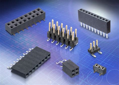
- Component Selection: Verify that all components (resistors, capacitors, ICs, etc.) are available, correctly specified, and have accurate footprints.
- Electrical Rules Check (ERC): Run an ERC to detect open connections, short circuits, or incorrect power ratings.
- Design Review: Collaborate with team members to confirm the schematic meets all functional requirements.
A well-validated schematic minimizes errors in the PCB layout phase.
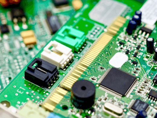
2. PCB Layout Optimization
The PCB layout determines signal integrity, thermal performance, and manufacturability. Key considerations include:
A. Layer Stackup Configuration
- Decide the number of layers (single-sided, double-sided, or multilayer) based on complexity.
- Define copper weights and dielectric materials for impedance control (critical for high-speed designs).
B. Component Placement
- Group related components (e.g., power supply sections, RF modules) to minimize trace lengths.
- Ensure proper spacing for heat dissipation, especially for high-power components.
- Consider mechanical constraints (enclosure size, connector positions).
C. Routing and Signal Integrity
- Follow best practices for trace width (based on current requirements).
- Avoid sharp angles in traces to prevent signal reflections.
- Implement proper grounding techniques (star grounding, ground planes) to reduce noise.
- Use differential pairs for high-speed signals (USB, HDMI, PCIe).
D. Design Rule Check (DRC)
Run a DRC to verify:
- Minimum trace spacing and width.
- Drill hole sizes and pad clearances.
- Copper-to-edge clearance (for panelization and assembly).
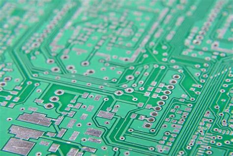
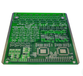
3. Generating Manufacturing Files
PCB manufacturers require specific file formats for fabrication. The standard files include:
- Gerber Files: Contains copper layers, solder mask, silkscreen, and drill data.
- NC Drill Files: Specifies hole sizes and locations.
- Bill of Materials (BOM): Lists all components with part numbers, quantities, and reference designators.
- Pick-and-Place File: Used for automated assembly (if applicable).
- Assembly Drawings: Provides visual guidance for component placement.
Ensure all files follow the manufacturer’s specifications (e.g., file naming conventions, layer ordering).
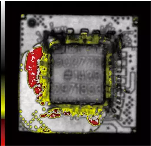
4. Design for Manufacturability (DFM) Review
A DFM review ensures the PCB can be fabricated without issues. Key aspects include:
- Minimum Trace/Space: Confirm compliance with the manufacturer’s capabilities.
- Hole Size and Aspect Ratio: Avoid excessively small vias that may not be drillable.
- Solder Mask and Silkscreen: Ensure legible text and proper mask openings for pads.
- Copper Balancing: Prevent warping by distributing copper evenly across layers.
Many manufacturers offer automated DFM checks, but manual verification is still recommended.
5. Selecting the Right PCB Manufacturer
Choosing a reliable manufacturer is critical. Factors to consider:
- Capabilities: Can they handle the required layer count, materials, and tolerances?
- Lead Time: Prototype lead times vary (from 24 hours to several weeks).
- Cost: Compare pricing for small-batch prototypes versus mass production.
- Certifications: ISO, UL, and IPC standards ensure quality compliance.
Request a quote and clarify any special requirements (e.g., impedance control, flexible PCBs).
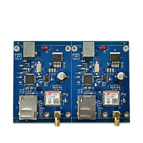
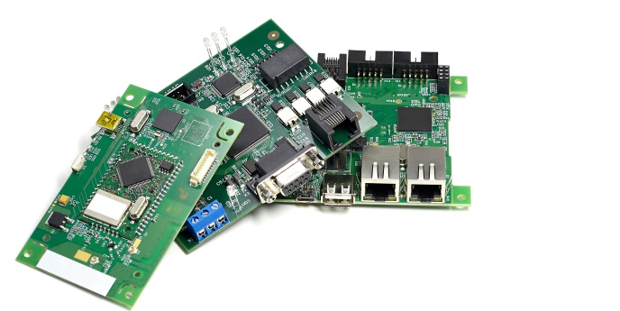
6. Prototype Testing and Validation Plan
Before mass production, prototypes must undergo rigorous testing:
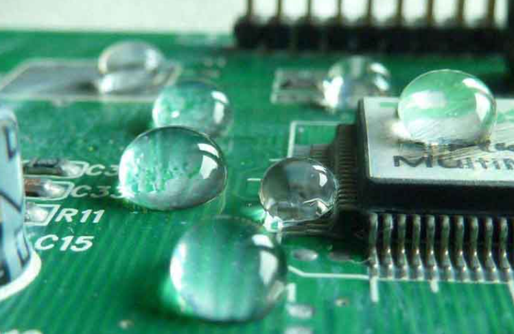
- Visual Inspection: Check for soldering defects, misaligned components, or physical damage.
- Continuity Testing: Verify no open or short circuits.
- Functional Testing: Power up the board and validate all circuits.
- Signal Integrity Analysis (if needed): Use oscilloscopes or network analyzers for high-speed designs.
Document all findings to refine the design in subsequent iterations.
7. Preparing for Revisions
Most PCB prototypes require multiple iterations. To streamline revisions:
- Version Control: Maintain a clear record of design changes.
- Feedback Loop: Gather input from testing teams and manufacturers.
- Cost Optimization: Identify areas where material or layout changes can reduce expenses.
Conclusion
Successful PCB prototyping requires meticulous preparation—from schematic validation to manufacturing file generation and DFM reviews. By following these steps, engineers can minimize errors, reduce costs, and accelerate product development. Investing time in thorough preparation ensures a smooth transition from prototype to full-scale production.
By adhering to these best practices, designers can confidently proceed with PCB fabrication, knowing their prototypes are optimized for performance, reliability, and manufacturability.