Express PCB: A Comprehensive Guide to Rapid PCB Prototyping
Introduction
Printed Circuit Boards (PCBs) are the backbone of modern electronics, providing the necessary connections between components in devices ranging from smartphones to industrial machinery. Designing and manufacturing PCBs traditionally required significant time and expertise, but tools like Express PCB have revolutionized the process by making it faster and more accessible.
Express PCB is a software and service solution that enables engineers, hobbyists, and businesses to design and order custom PCBs with ease. This article explores Express PCB’s features, benefits, workflow, and its role in rapid prototyping, providing a comprehensive guide for anyone interested in PCB design and manufacturing.
1. What is Express PCB?
Express PCB is a combination of PCB design software and a manufacturing service that simplifies the process of creating custom circuit boards. It offers:
- User-friendly PCB design tools for schematic capture and layout.
- Quick-turn manufacturing services with fast production and shipping.
- Affordable prototyping options for small batches.
Unlike complex CAD tools like Altium or KiCad, Express PCB is designed for simplicity, making it ideal for beginners and professionals who need quick results.
2. Key Features of Express PCB
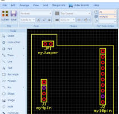
A. Intuitive Design Software
Express PCB provides a free, easy-to-use design tool with:
- Drag-and-drop component placement
- Automatic trace routing
- Real-time design rule checks (DRC)
- Schematic capture integration
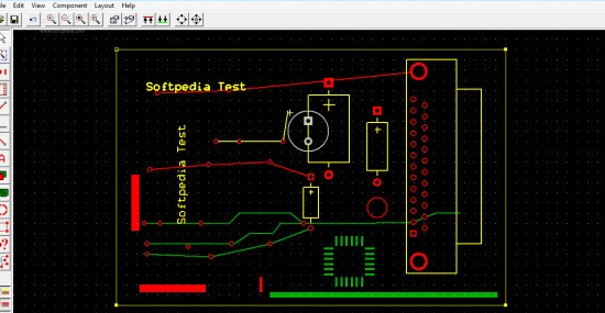
The software supports two-layer PCB designs, which are sufficient for many hobbyist and professional projects.
B. Fast Manufacturing Turnaround
One of the biggest advantages of Express PCB is its rapid production service:
- 24-hour turnaround for prototype orders (depending on complexity).
- Standard and expedited shipping options.
- High-quality fabrication with options for solder mask and silkscreen.
C. Affordable Prototyping
Express PCB offers cost-effective solutions for small batches:
- Low-cost prototypes (as few as three boards).
- No hidden fees—clear pricing based on board size and layer count.
- Discounts for students and educators.
D. Library of Components
The software includes a built-in component library with common parts, reducing the need for manual footprint creation. Users can also import custom components if needed.
3. How to Design a PCB Using Express PCB
Step 1: Schematic Design
- Open Express Schematic (included with Express PCB).
- Place components (resistors, ICs, connectors) from the library.
- Connect components using wires and nets.
- Verify the schematic for errors.
Step 2: PCB Layout
- Switch to Express PCB layout mode.
- Import the schematic to auto-place components (or place them manually).
- Route traces between components (auto-router available).
- Add power planes, vias, and test points as needed.
Step 3: Design Verification
- Run Design Rule Check (DRC) to detect spacing errors.
- Verify trace widths for current handling.
- Export Gerber files (for manufacturing elsewhere) or submit directly to Express PCB for production.
Step 4: Ordering PCBs
- Upload the design file to Express PCB’s website.
- Select board specifications (thickness, solder mask color, etc.).
- Choose shipping speed (standard or express).
- Receive PCBs in days (instead of weeks).
4. Advantages of Using Express PCB
A. Speed and Efficiency
- Faster than traditional PCB services (which can take weeks).
- No need for complex CAD training—ideal for quick projects.
B. Cost-Effective for Prototyping
- No minimum order quantity (MOQ)—order as few as three boards.
- Competitive pricing compared to other quick-turn services.
C. User-Friendly Interface
- Simpler than KiCad or Eagle for beginners.
- Good for educational purposes (students learning PCB design).
D. Reliable Manufacturing Quality
- High-quality FR-4 material.
- Professional-grade solder mask and silkscreen.
5. Limitations of Express PCB
While Express PCB is excellent for rapid prototyping, it has some limitations:
- Only supports 2-layer designs (no multi-layer PCBs).
- Limited advanced features (no high-speed signal analysis).
- Not suitable for very complex designs (better suited for Altium or Cadence).
For advanced users, combining Express PCB for quick prototypes and other tools for final production may be optimal.
6. Alternatives to Express PCB
While Express PCB is a great tool, alternatives include:
| Tool/Service | Pros | Cons |
|---|---|---|
| KiCad | Free, open-source, multi-layer support | Steeper learning curve |
| Eagle (Autodesk) | Powerful, widely used | Subscription-based, complex |
| OSH Park | Low-cost, community-driven | Slower turnaround |
| JLCPCB/PCBWay | Cheap, fast, global shipping | Requires Gerber file export |
7. Real-World Applications of Express PCB
Express PCB is widely used in:
- University projects (student electronics labs).
- Startup prototyping (IoT devices, wearables).
- Hobbyist electronics (Arduino shields, custom gadgets).
Example: A startup designing a smart sensor can use Express PCB to test multiple iterations quickly before mass production.
8. Future of Express PCB and Rapid Prototyping
As PCB manufacturing evolves, Express PCB may integrate:
- More layer support (4-layer designs).
- AI-assisted routing for faster design.
- 3D PCB preview for better visualization.
The demand for quick, affordable PCBs will continue to grow, making tools like Express PCB essential.
Conclusion
Express PCB is a powerful yet simple solution for fast, affordable PCB prototyping. Its intuitive software and quick-turn manufacturing make it ideal for hobbyists, students, and professionals who need reliable boards without long waits. While it has limitations for complex designs, it remains a top choice for rapid iteration and low-cost development.
For anyone entering PCB design, Express PCB provides an excellent balance of ease, speed, and quality, helping bring electronic ideas to life faster than ever.


