FinFETs drive smarter physical IP choices
The semiconductor industry is currently facing a dramatic change in the way integrated circuits (ICs) are manufactured, which is intended to continuously increase IC performance and density, and may have an impact on design methods. Foundries are currently preparing to enhance 14nm and 16nm processes using three-dimensional transistor structures based on the finFET concept because they can provide higher performance than 20nm planar transistors.
By increasing the current-carrying channel, the gate can be surrounded on three sides, allowing the gate to exhibit stronger electrostatic control. This overcomes short channel effects that lead to excessive leakage current and other problems caused by nanometer planar transistors made using large amounts of silicon.
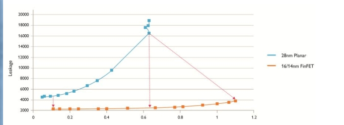
Figure 1: Better illustration of leakage current control over frequency
A further advantage of multi-level gating is that the drive current per unit area is more than that of a planar device – using the height of the fin structure can create a larger effective channel volume than a planar device for the same equivalent gate length. This means better effective performance.
By enhancing FinFET performance, higher frequency numbers can be achieved for a given power budget than bulk silicon technology.
The power reduction comes from two aspects: the reduced need for wide, high-drive standard cells and the ability to operate at lower supply voltages for a given amount of leakage current. However, the power reduction performance can only be fully realized by changing the design technology.
Standard cell-based flows remain the key to achieving high-productivity IC implementation.
Cell extraction has underpinned the foundation of synthesis-driven design flows for decades, providing the basis for highly automated digital circuit implementation, making it possible for small teams to design million-gate circuits. Changes in transistor structure and the associated layout-dependent effects are about to break through the clean interface between the physical, cell, and logic levels of the design flow, forcing designers to consider low-level features when laying out circuits. However, by increasing cell-level intelligence, the productivity benefits of standard cell extraction can be maintained and the power, performance, and area (PPA) benefits achieved by finFET-based processes can still be achieved.
With finFETs came a fundamental change in circuit structure due to its changed form factor (Figure 2). The fin structure for a given process has a fixed width and pitch. Compared to planar processes, where the overall drive strength can be increased by any amount to improve performance of large sectors or high capacitance buses, the effective width of a finFET can only be changed by adding more fins to the transistor. Fin quantization not only increases the complexity of analog and custom circuit design, but also has subtle but important effects on digital circuit implementation.
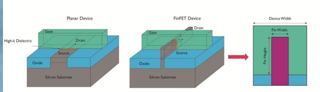
Figure 2: FinFET vs. planar transistor
In summary, finFET-based processes benefit from the narrowest possible fin pitch, as this will provide better density, flexibility, and performance. The process used to create the fins relies on chemically self-aligned technology that can achieve a pitch that is 25% smaller than the line pitch of the finest layers of metal interconnects (M1 and M2).
These metal layers are currently drawn using two independent masks that are combined into a composite exposure, rather than using a self-aligned process. The minimum pitch of these metal layers is determined by the overlay error, so the higher pitch can be achieved using a self-aligned fin formation step.
When designing standard cells that implement the bulk of the digital logic that will be used in finFET-based ICs, the mismatch between the fins and the M2 pitch needs to be accounted for (typically, the fins are parallel to the M2 pitch).
For finFET-based processes, there are only a few effective “gear ratios” between the fins and the metal wire pitch that produce a viable standard cell library, so they need to be designed so that each cell has a fixed number of routing paths.
Even so, some combinations result in an inflexible metal grid that makes it difficult to carry enough current for cells on critical paths. Nano processes are increasingly subject to effects such as electromigration, which thins and eventually vanishes metal wires that carry high currents, shortening the lifecycle of ICs.

For maximum metal routing density, the two-mask design rule applies not only to the metal wire pitch, but also to its width.
The result is that wider metal wires cannot always be drawn to carry the high currents required to provide cells with high drive power. Certain ratios of fin count to metal wire count allow for more flexibility in the use of metal interconnect processes when routing power. They allow for wider, more flexible power rails when needed, while the number of routing paths in the cell allows for higher logic routing density to carry power. Taking advantage of this structure requires a deeper understanding of the standard cell architecture beyond what is known from traditional place-and-route tools, which are designed to use the standard cell as a black box with a set of I/O and power pins in predetermined locations.
Tools that can use their understanding of the internal standard cell architecture and remap the cell as needed for logic can provide the additional flexibility needed to take advantage of this new structure without completely restructuring the IC implementation process. The same understanding can help other design flows adopt the latest design changes, resulting in engineering change orders (ECOs).
As design rules become more restrictive than ever before, implementing ECOs has become more difficult because even a small change can cause issues with mask colors in dual-pattern layers.

Flows that incorporate tools that understand the local standard cell environment can go deeper into the design to implement ECOs as transparently as possible.
A deep understanding of the internal architecture of the standard cell will help address other issues that arise from migrating to finFET-based nanometer processes. As designers try to exploit the higher performance of 3D transistors and increase clock speeds, they will encounter more severe variability challenges. Although finFETs exhibit lower variability than planar transistors in some key metrics, variability is still a major obstacle to timing termination and exists in many ways across the boundaries between standard cells and routing layers.
Traditionally, such variability would be integrated into guard bands that limit clock speeds, hindering the performance gains achieved with finFET structures. Better analysis and correction techniques can largely recover this performance loss, thereby increasing clock speeds and making products more competitive in the market.
It has been proven that the dual-patterning techniques used in finFET-based processes at 14nm and 16nm can cause large differences in path delays.
For example, a small shift in aligning one of the masks used to image the interconnect pattern can increase the coupling capacitance between the gate electrode and the cable, thereby increasing the path delay. Because the shift will be consistent across the mask, the delay of the transistor associated with that mask pattern can be correlated – and more advanced analysis tools that understand the behavior and internal connectivity of each standard cell can also take it into account. By considering the above correlations and taking corrective actions, it is possible to eliminate concerns about coupling capacitance differences and increase target clock speeds.
Interconnect parasitics, especially the high resistance of metal wires in finFET-based processes, will also hinder clock tree performance.
Clock trees use a large number of long-distance connections to keep the timing of the IC consistent. Traditional techniques such as buffer insertion will increase power consumption. By applying knowledge of basic standard cells, smarter clock tree optimization can be performed to provide low-skew timing signals and avoid blowing power budgets.
Reducing device geometry also increases the likelihood of single event upsets due to ionizing radiation, which can lead to incorrect results and system crashes. Analyzing cell structures in the context of the circuit (and potentially replacing them with enhanced versions) can reduce the likelihood of improper behavior in the presence of alpha particles.
The move to finFET-based processes will bring about a large number of process-level changes and impacts on digital design. If not addressed, it will lead to poor IC performance. While these physical effects have the potential to threaten extremely stable, standard cell-based processes, the availability of tools that address SoC design at the cell level will help maintain process stability and fully realize the benefits of finFET-based processes.