Flex pcb layer stackup
Understanding The Basics Of Flex PCB Layer Stackup
Flex PCB layer stackup is a critical aspect of designing flexible printed circuit boards, which are increasingly used in modern electronics due to their versatility and ability to conform to complex shapes.
Understanding the basics of flex PCB layer stackup is essential for engineers and designers aiming to optimize the performance and reliability of their electronic devices.
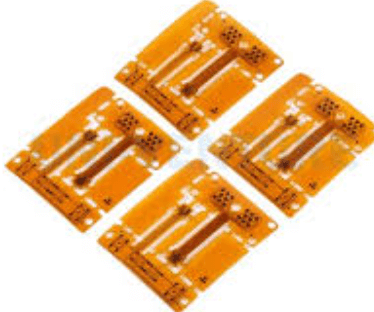
To begin with, a flex PCB, or flexible printed circuit board, is a type of PCB that can bend and flex, unlike traditional rigid PCBs.
This flexibility is achieved through the use of flexible base materials such as polyimide or polyester films, which provide the necessary mechanical properties. The layer stackup of a flex PCB refers to the arrangement and sequence of conductive and insulating layers that make up the board. This stackup is crucial because it directly impacts the electrical performance, mechanical durability, and manufacturability of the PCB.
In a typical flex PCB layer stackup, the core layer is usually a flexible dielectric material, such as polyimide, which provides the foundational support for the circuit.
On either side of this core layer, conductive layers made of copper are added. These copper layers form the electrical pathways that connect various components on the PCB. The number of conductive layers can vary depending on the complexity of the circuit, ranging from a single layer to multiple layers in more advanced designs.
To ensure electrical insulation between the conductive layers, dielectric layers are inserted between them.
These dielectric layers are also made of flexible materials and play a crucial role in maintaining the integrity of the electrical signals. Additionally, coverlays or cover films are often applied to the outermost layers of the flex PCB. These coverlays protect the copper traces from environmental factors such as moisture, dust, and mechanical abrasion, thereby enhancing the durability of the PCB.
Transitioning to the design considerations, the thickness of each layer in the stackup must be carefully controlled.
The overall thickness of the flex PCB affects its flexibility and bend radius. A thinner PCB will be more flexible but may be less durable, while a thicker PCB will be more robust but less flexible. Therefore, designers must strike a balance between flexibility and durability based on the specific application requirements.
Moreover, the choice of materials for each layer is another critical factor.
The dielectric constant and loss tangent of the insulating materials influence the signal integrity and impedance control of high-frequency circuits. Similarly, the type of copper used, whether rolled annealed (RA) or electrodeposited (ED), affects the mechanical properties and performance of the flex PCB. RA copper is preferred for applications requiring high flexibility and dynamic bending, while ED copper is suitable for static applications.
Manufacturing processes also play a significant role in the final quality of the flex PCB.
Techniques such as adhesive bonding, lamination, and etching must be precisely controlled to ensure that the layers are properly aligned and bonded. Any misalignment or defects in the stackup can lead to electrical failures or mechanical issues.
In conclusion, understanding the basics of flex PCB layer stackup is fundamental for designing reliable and high-performance flexible circuits. By carefully considering the arrangement, materials, and manufacturing processes, designers can create flex PCBs that meet the specific needs of their applications while ensuring optimal performance and durability. As technology continues to advance, the importance of mastering flex PCB layer stackup will only grow, making it a vital skill for modern electronics engineers.
Key Considerations For Designing Flex PCB Layer Stackup
When designing a flex PCB layer stackup, several key considerations must be taken into account to ensure optimal performance and reliability.
The first aspect to consider is the material selection.
Flex PCBs typically use polyimide as the base material due to its excellent thermal stability, flexibility, and dielectric properties. However, the choice of adhesive and copper foil also plays a crucial role.
Adhesives must be chosen based on their thermal and mechanical properties, while the copper foil should be selected for its thickness and ductility to withstand bending and flexing.
Another critical factor is the number of layers in the stackup.
Flex PCBs can range from single-layer to multi-layer configurations, depending on the complexity of the circuit. Single-layer flex PCBs are simpler and less expensive but may not provide the necessary routing options for more complex designs. Multi-layer flex PCBs, on the other hand, offer greater design flexibility and can accommodate more intricate circuits. However, they are more challenging to manufacture and can be more costly.
The next consideration is the bend radius, which is the minimum radius that the flex PCB can be bent without causing damage.
The bend radius is influenced by the thickness of the PCB and the materials used. A smaller bend radius allows for more compact designs but increases the risk of mechanical failure. Therefore, it is essential to balance the need for compactness with the mechanical limitations of the materials.
Thermal management is another important aspect of flex PCB design.
Flex PCBs are often used in applications where heat dissipation is a concern, such as in automotive or aerospace industries. Proper thermal management ensures that the PCB can operate reliably under varying temperature conditions. This can be achieved through the use of thermal vias, heat sinks, and careful placement of components to distribute heat evenly.
Signal integrity is also a crucial consideration, especially for high-speed applications.
The design of the layer stackup can significantly impact signal integrity. Factors such as trace width, spacing, and the use of ground planes must be carefully considered to minimize signal loss and electromagnetic interference. Additionally, the dielectric constant of the materials used can affect signal propagation, so it is important to choose materials with suitable electrical properties.
Manufacturability is another key consideration.
The design of the flex PCB layer stackup must take into account the capabilities and limitations of the manufacturing process. This includes considerations such as the minimum trace width and spacing, the ability to drill vias, and the precision of the etching process. Working closely with the manufacturer during the design phase can help identify potential issues and ensure that the design can be produced reliably and cost-effectively.
Finally, reliability and durability are paramount in flex PCB design.
The flex PCB must be able to withstand repeated bending and flexing without failure. This requires careful selection of materials, as well as thorough testing and validation of the design. Environmental factors such as humidity, temperature, and exposure to chemicals must also be considered, as they can affect the long-term performance of the PCB.
In conclusion, designing a flex PCB layer stackup involves a complex interplay of material selection, mechanical design, thermal management, signal integrity, manufacturability, and reliability. By carefully considering each of these factors, designers can create flex PCBs that meet the specific requirements of their applications while ensuring optimal performance and durability.

Common Challenges In Flex PCB Layer Stackup And How To Overcome Them
Flex PCB layer stackup is a critical aspect of designing flexible printed circuit boards, which are increasingly used in various applications due to their versatility and space-saving benefits.
However, the process of creating an effective layer stackup for flex PCBs is fraught with challenges that can impact the performance, reliability, and manufacturability of the final product. Understanding these common challenges and knowing how to overcome them is essential for engineers and designers working in this field.
One of the primary challenges in flex PCB layer stackup is managing the mechanical stress that the board will experience during its lifecycle.
Flex PCBs are often subjected to bending, twisting, and other forms of mechanical deformation, which can lead to issues such as delamination, cracking, or even complete failure of the circuit. To mitigate these risks, it is crucial to carefully select materials that offer the right balance of flexibility and durability. Polyimide is a popular choice for flex PCBs due to its excellent thermal stability and mechanical properties. Additionally, incorporating strain relief features, such as curved traces and filleted corners, can help distribute mechanical stress more evenly across the board.
Another significant challenge is ensuring signal integrity in high-speed applications.
As the demand for faster data transmission rates continues to grow, maintaining signal integrity becomes increasingly important. Flex PCBs can be particularly susceptible to issues such as crosstalk, impedance mismatches, and signal attenuation due to their unique structure and the materials used. To address these concerns, designers must pay close attention to the stackup configuration, ensuring that the signal and ground layers are properly arranged to minimize electromagnetic interference. Utilizing controlled impedance techniques and incorporating ground planes can also help maintain signal integrity.
Thermal management is another critical aspect of flex PCB layer stackup design.
Flexible circuits are often used in compact and densely populated electronic devices, where heat dissipation can be a significant concern. Poor thermal management can lead to overheating, which can degrade the performance and reliability of the components. To overcome this challenge, designers can use materials with high thermal conductivity, such as thermally conductive adhesives and substrates. Additionally, incorporating thermal vias and heat sinks can help dissipate heat more effectively, ensuring that the flex PCB operates within safe temperature limits.
Manufacturability is also a key consideration when designing flex PCB layer stackups.
The unique properties of flexible materials can pose challenges during the fabrication process, such as difficulties in handling, alignment, and lamination. To ensure a smooth manufacturing process, it is essential to work closely with experienced PCB fabricators who are familiar with the intricacies of flex PCB production. Designing with manufacturability in mind, such as optimizing the layer stackup for ease of fabrication and assembly, can help minimize production issues and reduce costs.
In conclusion, while designing flex PCB layer stackups presents several challenges, understanding these issues and implementing appropriate strategies can significantly enhance the performance, reliability, and manufacturability of the final product. By carefully selecting materials, managing mechanical stress, ensuring signal integrity, addressing thermal management, and considering manufacturability, designers can overcome these challenges and create robust and efficient flex PCBs for a wide range of applications.
Innovations And Trends In Flex PCB Layer Stackup Technology
Flex PCB layer stackup technology has undergone significant advancements in recent years, driven by the increasing demand for more compact, reliable, and versatile electronic devices. As the electronics industry continues to evolve, innovations in flex PCB layer stackup are playing a crucial role in meeting the stringent requirements of modern applications.
One of the most notable trends in this domain is the development of multi-layer flex PCBs,
which offer enhanced functionality and performance compared to their single-layer counterparts. By incorporating multiple layers of conductive material separated by insulating layers, these advanced PCBs can support more complex circuitry and higher component densities, making them ideal for use in sophisticated electronic devices such as smartphones, medical equipment, and automotive systems.
In addition to the rise of multi-layer flex PCBs, there has been a growing emphasis on the use of advanced materials to improve the performance and reliability of these flexible circuits.
For instance, the adoption of high-performance polyimide films as the base material for flex PCBs has become increasingly common. Polyimide films offer excellent thermal stability, chemical resistance, and mechanical strength, making them well-suited for demanding applications where traditional materials may fall short. Furthermore, the use of advanced adhesives and bonding techniques has enabled the creation of more robust and durable flex PCBs, capable of withstanding harsh environmental conditions and mechanical stress.
Another key innovation in flex PCB layer stackup technology is the integration of rigid-flex PCBs, which combine the benefits of both rigid and flexible circuits.
Rigid-flex PCBs consist of rigid sections connected by flexible interconnects, allowing for greater design flexibility and improved performance in applications where space constraints and mechanical stress are significant concerns. This hybrid approach enables the creation of more compact and reliable electronic devices, as it allows for the integration of complex circuitry within a smaller footprint while maintaining the necessary mechanical support and stability.
Moreover, advancements in manufacturing processes have also contributed to the evolution of flex PCB layer stackup technology.
The adoption of laser drilling and precision etching techniques has enabled the production of finer and more intricate circuit patterns, allowing for higher component densities and improved electrical performance. Additionally, the use of automated assembly and inspection processes has enhanced the overall quality and consistency of flex PCBs, reducing the likelihood of defects and ensuring that these advanced circuits meet the stringent requirements of modern applications.
As the demand for more compact and reliable electronic devices continues to grow, the importance of innovations in flex PCB layer stackup technology cannot be overstated.
The development of multi-layer flex PCBs, the use of advanced materials, the integration of rigid-flex designs, and advancements in manufacturing processes are all contributing to the creation of more sophisticated and high-performance electronic devices. These innovations are not only enabling the development of new and exciting applications but are also helping to drive the overall progress of the electronics industry.
In conclusion, the ongoing advancements in flex PCB layer stackup technology are playing a pivotal role in shaping the future of electronic devices. By embracing new materials, manufacturing techniques, and design approaches, the industry is continually pushing the boundaries of what is possible, paving the way for more compact, reliable, and versatile electronic solutions. As these trends continue to evolve, it is clear that flex PCB layer stackup technology will remain at the forefront of innovation, driving the next generation of electronic devices and applications.
.