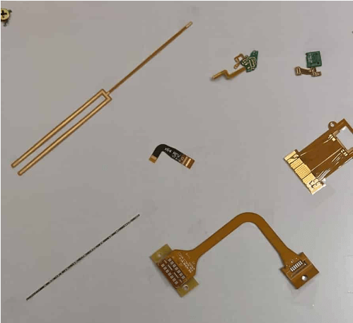
Flex pcb strain relief
Benefits Of Flex PCB Strain Relief In High-Stress Environments
Flex PCB strain relief is a critical consideration in the design and application of flexible printed circuit boards, particularly in high-stress environments. These environments, characterized by constant mechanical stress, temperature fluctuations, and potential exposure to harsh chemicals, demand robust solutions to ensure the longevity and reliability of electronic components. The implementation of strain relief mechanisms in flex PCBs offers numerous benefits that enhance their performance and durability under such demanding conditions.
One of the primary advantages of incorporating strain relief in flex PCBs is the significant reduction in mechanical stress on the circuit traces and solder joints.
Flexible circuits are often subjected to bending, twisting, and stretching, which can lead to the development of micro-cracks and eventual failure of the conductive pathways. By integrating strain relief features, such as strategically placed stiffeners or the use of more flexible materials at critical points, the mechanical load is distributed more evenly across the board. This distribution minimizes the concentration of stress at any single point, thereby extending the operational life of the PCB.
In addition to mitigating mechanical stress, strain relief in flex PCBs also enhances their thermal stability.
High-stress environments often involve significant temperature variations, which can cause expansion and contraction of the materials used in the PCB. These thermal cycles can exacerbate mechanical stresses and lead to delamination or other forms of structural failure. Strain relief designs that account for thermal expansion properties help maintain the integrity of the PCB by allowing for controlled movement and reducing the risk of damage due to thermal cycling.
Moreover, the use of strain relief in flex PCBs contributes to improved electrical performance.
Mechanical stress and thermal cycling can adversely affect the electrical properties of the circuit, leading to issues such as increased resistance, signal degradation, and potential short circuits. By alleviating these stresses, strain relief ensures that the electrical characteristics of the PCB remain stable over time, which is crucial for maintaining the reliability of high-performance electronic systems.
Another significant benefit of flex PCB strain relief is its role in enhancing the overall durability and reliability of electronic devices.
In high-stress environments, electronic components are often exposed to vibrations, shocks, and other forms of physical impact. Strain relief features help absorb and dissipate these forces, protecting the delicate circuitry from damage. This protection is particularly important in applications such as aerospace, automotive, and industrial machinery, where failure of electronic components can have severe consequences.
Furthermore, the implementation of strain relief in flex PCBs can lead to cost savings in the long run.
While the initial design and manufacturing process may be more complex and potentially more expensive, the extended lifespan and improved reliability of the PCB can result in lower maintenance costs and reduced downtime. This cost-effectiveness is especially valuable in high-stress environments where equipment failure can lead to significant operational disruptions and financial losses.
In conclusion, the benefits of flex PCB strain relief in high-stress environments are manifold. By reducing mechanical stress, enhancing thermal stability, improving electrical performance, and increasing overall durability, strain relief mechanisms play a crucial role in ensuring the reliability and longevity of flexible printed circuit boards. As technology continues to advance and the demand for robust electronic solutions grows, the importance of effective strain relief in flex PCBs will only become more pronounced, making it an essential consideration for designers and engineers working in high-stress applications.
Techniques For Implementing Effective Flex PCB Strain Relief
Flex PCB strain relief is a critical aspect of designing flexible printed circuit boards, ensuring their longevity and reliability in various applications. As electronic devices become increasingly compact and complex, the demand for flexible PCBs has surged, necessitating effective techniques to mitigate strain and prevent damage. Implementing strain relief in flex PCBs involves a combination of design strategies and material choices, each contributing to the overall durability and performance of the circuit.
One fundamental technique for achieving effective strain relief in flex PCBs is the incorporation of bend radii.
By designing the PCB with appropriate bend radii, engineers can distribute mechanical stress more evenly across the board, reducing the likelihood of cracks or fractures. Typically, a larger bend radius is preferred, as it minimizes the concentration of stress at any single point. This approach is particularly important in applications where the PCB will undergo repeated flexing or bending, such as in wearable electronics or foldable devices.
In addition to bend radii, the use of stiffeners is another crucial method for strain relief.
Stiffeners are rigid materials, often made of polyimide or FR4, that are attached to specific areas of the flex PCB to provide additional support and rigidity. By reinforcing these areas, stiffeners help to prevent excessive bending and flexing, thereby reducing the risk of mechanical failure. Stiffeners are commonly used around connectors, mounting points, and other critical regions where mechanical stress is likely to be concentrated.
Moreover, the choice of materials plays a significant role in enhancing strain relief.
Flexible PCBs are typically constructed from materials such as polyimide, which offers excellent flexibility and thermal stability. However, selecting the right adhesive and coverlay materials is equally important. High-quality adhesives ensure a strong bond between the layers of the PCB, while durable coverlays protect the circuitry from environmental factors and mechanical wear. By carefully selecting these materials, engineers can enhance the overall resilience of the flex PCB.
Another effective technique involves the strategic placement of traces and components.
By routing traces along the neutral axis of the flex PCB, where the stress is minimal during bending, engineers can further reduce the risk of damage. Additionally, placing components away from high-stress areas and ensuring even distribution of weight can help to minimize mechanical strain. This approach not only enhances the durability of the PCB but also improves its electrical performance by reducing the likelihood of signal interference or degradation.
Furthermore, the implementation of strain relief features such as fillets and teardrops can significantly enhance the robustness of flex PCBs.
Fillets are rounded transitions between traces and pads, which help to distribute stress more evenly and prevent stress concentration at sharp corners. Teardrops, on the other hand, are gradual transitions between traces and vias, reducing the risk of cracking at these junctions. By incorporating these features into the design, engineers can improve the mechanical integrity of the flex PCB.
In conclusion, effective flex PCB strain relief is achieved through a combination of design strategies and material choices. By incorporating appropriate bend radii, using stiffeners, selecting high-quality materials, strategically placing traces and components, and implementing strain relief features such as fillets and teardrops, engineers can significantly enhance the durability and reliability of flexible printed circuit boards. As the demand for flexible electronics continues to grow, these techniques will play an increasingly vital role in ensuring the performance and longevity of flex PCBs in a wide range of applications.
Common Mistakes To Avoid In Flex PCB Strain Relief Design
In the realm of flexible printed circuit boards (flex PCBs), strain relief design is a critical aspect that ensures the longevity and reliability of the circuit. However, several common mistakes can undermine the effectiveness of strain relief, leading to premature failure and costly repairs.
One prevalent error is the improper placement of strain relief features.
Designers often overlook the importance of positioning these features at points where the flex PCB is most likely to experience mechanical stress. This oversight can result in concentrated stress points that accelerate wear and tear, ultimately compromising the integrity of the circuit.
Another frequent mistake is the use of inadequate materials for strain relief.
The choice of materials plays a pivotal role in the performance of flex PCBs under stress. Utilizing materials that lack the necessary flexibility or durability can lead to cracking and delamination. It is essential to select materials that can withstand repeated bending and flexing without degrading. Additionally, the thickness of the flex PCB should be carefully considered. A design that is too thin may not provide sufficient support, while one that is too thick can be overly rigid, negating the benefits of a flexible circuit.
Transitioning to the layout design, improper routing of traces is another common pitfall.
Traces that are routed too close to the edges of the flex PCB are more susceptible to damage from bending and flexing. To mitigate this risk, traces should be routed with adequate clearance from the edges and should follow smooth, curved paths rather than sharp angles. This approach helps distribute mechanical stress more evenly across the flex PCB, reducing the likelihood of trace breakage.
Furthermore, neglecting to incorporate adequate support structures can significantly impact the effectiveness of strain relief.
Support structures, such as stiffeners and strain relief pads, provide additional mechanical support to areas of the flex PCB that are prone to stress. Without these structures, the flex PCB is more vulnerable to mechanical failure. It is crucial to strategically place these supports in areas where the flex PCB interfaces with connectors or other rigid components, as these are common points of stress concentration.
In addition to these design considerations, it is also important to account for the environmental conditions in which the flex PCB will operate.
Factors such as temperature fluctuations, humidity, and exposure to chemicals can all influence the performance of strain relief features. Failing to consider these environmental factors can lead to the selection of inappropriate materials and designs that are not robust enough to withstand the operating conditions. Therefore, a thorough understanding of the application environment is essential for effective strain relief design.
Lastly, inadequate testing and validation of the strain relief design can result in unforeseen failures.
Comprehensive testing, including mechanical stress tests and environmental simulations, is necessary to validate the effectiveness of the strain relief features. Skipping these critical steps can lead to the deployment of flex PCBs that are not fully optimized for their intended use, increasing the risk of failure in the field.
In conclusion, avoiding these common mistakes in flex PCB strain relief design requires careful consideration of material selection, trace routing, support structures, environmental conditions, and thorough testing. By addressing these factors, designers can enhance the durability and reliability of flex PCBs, ensuring they perform optimally in their intended applications.
Innovations In Flex PCB Strain Relief Materials And Methods
Flex PCBs, or flexible printed circuit boards, have become increasingly integral to modern electronics due to their versatility, lightweight nature, and ability to conform to various shapes. However, one of the critical challenges in their application is ensuring strain relief. Strain relief is essential to prevent mechanical stress from damaging the delicate circuitry, which can lead to failures and reduced longevity of the device. Innovations in materials and methods for flex PCB strain relief have been pivotal in addressing these challenges, enhancing the reliability and performance of electronic devices.
One of the primary advancements in this field is the development of advanced polymer materials.
Traditional materials often lacked the necessary flexibility and durability, leading to premature wear and tear. However, recent innovations have introduced high-performance polymers that offer superior mechanical properties. These materials can withstand repeated bending and flexing without compromising the integrity of the circuit. For instance, polyimide films have gained popularity due to their excellent thermal stability and mechanical strength. These films provide a robust yet flexible substrate that can endure the rigors of dynamic applications.
In addition to material advancements, innovative manufacturing techniques have also played a crucial role in improving strain relief for flex PCBs.
Laser direct structuring (LDS) is one such technique that has revolutionized the production process. LDS allows for the precise creation of circuit patterns directly onto the flexible substrate, eliminating the need for additional layers that could introduce stress points. This method not only enhances the overall flexibility of the PCB but also reduces the risk of mechanical failure by minimizing potential weak spots.
Moreover, the integration of strain relief features during the design phase has become increasingly sophisticated.
Engineers now employ finite element analysis (FEA) to simulate and predict the behavior of flex PCBs under various stress conditions. This predictive modeling enables the identification of potential failure points and allows for the optimization of the PCB layout to distribute stress more evenly. By incorporating these insights into the design, manufacturers can create more resilient flex PCBs that are better equipped to handle mechanical strain.
Another noteworthy innovation is the use of encapsulation techniques to provide additional protection to flex PCBs.
Encapsulation involves coating the PCB with a protective layer that shields it from environmental factors such as moisture, dust, and mechanical stress. Advanced encapsulation materials, such as silicone gels and conformal coatings, offer excellent flexibility and adhesion properties. These materials can conform to the intricate shapes of flex PCBs, providing a seamless protective barrier that enhances durability and reliability.
Furthermore, the adoption of hybrid flex-rigid PCBs has emerged as a promising solution for applications requiring both flexibility and rigidity.
These hybrid designs combine flexible and rigid sections within a single PCB, allowing for greater design flexibility and improved strain relief. The rigid sections provide structural support and stability, while the flexible sections enable dynamic movement and bending. This combination ensures that the PCB can withstand mechanical stress without compromising its functionality.
In conclusion, the continuous advancements in materials and methods for flex PCB strain relief have significantly improved the reliability and performance of electronic devices. The development of high-performance polymers, innovative manufacturing techniques, sophisticated design approaches, advanced encapsulation methods, and hybrid flex-rigid designs have all contributed to enhancing the durability and longevity of flex PCBs. As technology continues to evolve, these innovations will undoubtedly play a crucial role in meeting the growing demands of modern electronics, ensuring that flex PCBs remain a cornerstone of cutting-edge device design.