Flex rigid pcb kicad
Introduction To Flex Rigid PCB Design In KiCad
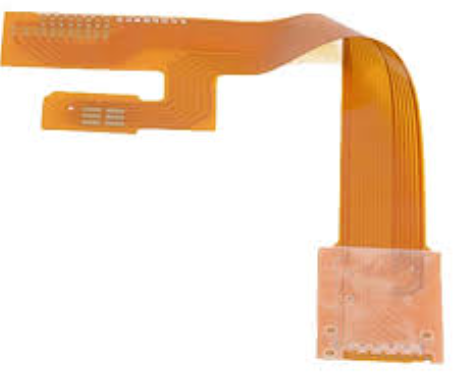
Flex rigid PCBs, a hybrid of flexible and rigid circuit boards, have become increasingly popular in modern electronics due to their versatility and reliability. These boards combine the best of both worlds, offering the flexibility needed for complex designs and the rigidity required for stable component mounting.
KiCad, an open-source electronic design automation (EDA) tool, provides a robust platform for designing flex rigid PCBs. This article introduces the fundamental concepts of flex rigid PCB design in KiCad, guiding you through the essential steps and considerations.
To begin with, understanding the structure of flex rigid PCBs is crucial.
These boards typically consist of multiple layers, with some layers being flexible and others rigid. The flexible layers allow the board to bend and twist, making them ideal for applications where space constraints or mechanical movement are factors. The rigid sections, on the other hand, provide a solid foundation for mounting components and connectors. This combination enhances the overall functionality and durability of the electronic device.
When designing a flex rigid PCB in KiCad, the first step is to set up the project correctly.
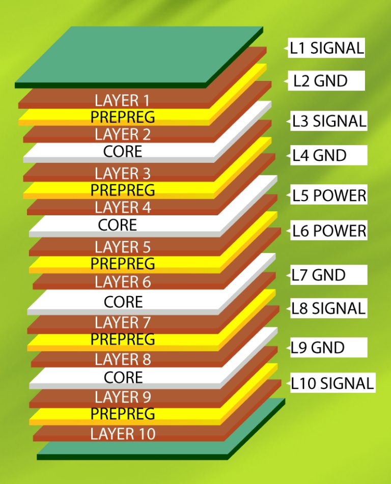
This involves defining the stack-up, which specifies the arrangement and materials of the different layers. KiCad allows you to customize the stack-up to match the specific requirements of your design. You can define the number of layers, their thickness, and the materials used, ensuring that the final product meets the necessary mechanical and electrical specifications.
Next, it is essential to create a detailed schematic of the circuit.
KiCad’s schematic editor provides a comprehensive set of tools for drawing and annotating the circuit diagram. This step involves placing components, drawing connections, and assigning net names. Properly organizing the schematic is vital, as it directly influences the layout process. Using hierarchical sheets can help manage complex designs by breaking them down into smaller, more manageable sections.
Once the schematic is complete, the next phase is the layout design.
KiCad’s PCB editor is equipped with features specifically tailored for flex rigid PCB design. One of the key aspects to consider during this phase is the placement of components. It is important to strategically place components on the rigid sections to ensure stability and reliability. The flexible sections should be reserved for areas that require bending or movement. Additionally, careful routing of traces is necessary to avoid stress points that could lead to mechanical failure.
KiCad also offers tools for defining the board outline and creating cutouts, which are essential for flex rigid designs.
The board outline defines the shape and size of the PCB, while cutouts allow for the separation of flexible and rigid sections. These features enable designers to create intricate shapes and ensure that the board fits perfectly within the intended enclosure.
Another critical aspect of flex rigid PCB design is the use of vias and pads.
Vias are used to connect different layers of the PCB, and their placement must be carefully considered to avoid compromising the board’s flexibility. Pads, on the other hand, provide the connection points for components and connectors. KiCad allows you to customize the size and shape of vias and pads, ensuring that they meet the specific requirements of your design.
In conclusion, designing flex rigid PCBs in KiCad involves a series of well-defined steps, from setting up the project and creating the schematic to designing the layout and defining the board outline. By leveraging KiCad’s powerful tools and features, designers can create highly reliable and versatile flex rigid PCBs that meet the demands of modern electronic applications. Understanding the unique requirements of flex rigid designs and carefully planning each step of the process are key to achieving a successful outcome.
Benefits Of Using Flex Rigid PCBs In Modern Electronics
Flex rigid PCBs, or flexible-rigid printed circuit boards, have become increasingly prevalent in modern electronics due to their unique combination of flexibility and rigidity. These hybrid circuits integrate flexible and rigid substrates into a single board, offering a multitude of benefits that cater to the evolving demands of contemporary electronic devices.
As the electronics industry continues to push the boundaries of innovation, the advantages of using flex rigid PCBs are becoming more apparent, particularly when designed using advanced tools like KiCad.
One of the primary benefits of flex rigid PCBs is their ability to save space and reduce weight.
Traditional rigid PCBs can be bulky and cumbersome, especially in applications where space is at a premium. By incorporating flexible sections, designers can create more compact and lightweight devices without compromising on functionality. This is particularly advantageous in the development of portable electronics, such as smartphones, tablets, and wearable technology, where every millimeter and gram counts.
In addition to space-saving benefits, flex rigid PCBs offer enhanced reliability and durability.
The flexible sections of these boards can withstand bending and flexing, which reduces the risk of damage from mechanical stress. This makes them ideal for applications that require frequent movement or are subject to vibrations, such as automotive and aerospace industries. The rigid sections, on the other hand, provide a stable platform for mounting components, ensuring that the overall integrity of the circuit is maintained.
Another significant advantage of flex rigid PCBs is their ability to simplify complex designs.
By integrating multiple rigid and flexible layers into a single board, designers can eliminate the need for connectors and cables that would otherwise be required to link separate rigid boards. This not only reduces the overall complexity of the design but also minimizes potential points of failure, leading to improved performance and reliability. Furthermore, the use of flex rigid PCBs can streamline the manufacturing process, as fewer components and assembly steps are needed.
The design and development of flex rigid PCBs have been greatly facilitated by advanced electronic design automation (EDA) tools like KiCad.
KiCad is an open-source software suite that provides a comprehensive set of tools for PCB design, including schematic capture, PCB layout, and 3D visualization. With its robust feature set and user-friendly interface, KiCad enables designers to create intricate flex rigid PCB designs with ease. The software supports the creation of multi-layer boards, allowing for the integration of both flexible and rigid sections within a single design. Additionally, KiCad’s extensive library of components and footprints ensures that designers have access to the necessary resources to bring their designs to life.
Moreover, the use of KiCad in designing flex rigid PCBs can lead to cost savings.
AS an open-source tool, KiCad is freely available, eliminating the need for expensive licensing fees associated with proprietary EDA software. This makes it an attractive option for startups and small businesses looking to develop cutting-edge electronic products without incurring significant costs. Additionally, the active community of KiCad users and developers provides a wealth of knowledge and support, further enhancing the design process.
In conclusion, the benefits of using flex rigid PCBs in modern electronics are manifold. From space and weight savings to enhanced reliability and simplified designs, these hybrid circuits offer a versatile solution for a wide range of applications. The use of advanced design tools like KiCad further amplifies these advantages, making the development of flex rigid PCBs more accessible and cost-effective. As the demand for innovative electronic devices continues to grow, the adoption of flex rigid PCBs is poised to play a crucial role in shaping the future of the industry.

Step-By-Step Guide To Creating Flex Rigid PCBs In KiCad
Creating flex rigid PCBs in KiCad involves a series of methodical steps that ensure the design meets both functional and manufacturability requirements. To begin with, it is essential to understand that flex rigid PCBs combine flexible and rigid substrates into a single board, offering both flexibility and durability. This hybrid nature makes them ideal for applications where space constraints and mechanical stress are significant considerations.
The first step in designing a flex rigid PCB in KiCad is to set up the project environment.
Open KiCad and create a new project. This will generate a project directory containing essential files. Next, configure the project settings to match the specifications of your flex rigid PCB. This includes defining the number of layers, the type of materials to be used, and the stack-up configuration. It is crucial to consult with your PCB manufacturer to ensure that your design parameters align with their capabilities.
Once the project is set up, the next step is to create the schematic.
In the schematic editor, place the components required for your design. Ensure that each component is correctly annotated and that the electrical connections are accurately represented. Use the electrical rules check (ERC) feature to verify that there are no errors in the schematic. This step is vital as it ensures that the design will function as intended.
After completing the schematic, proceed to the PCB layout editor.
Import the netlist generated from the schematic to begin placing components on the board. At this stage, it is essential to define the rigid and flexible regions of the PCB. This can be done by creating separate zones for each region and specifying the appropriate layer stack-up for each zone. Use the layer manager to assign different materials and thicknesses to the rigid and flexible sections.
Routing the traces is the next critical step.
Start by routing the high-speed and critical signals, ensuring that they follow the shortest and most direct paths. For the flexible regions, use curved traces instead of sharp angles to prevent stress points that could lead to mechanical failure. Additionally, consider using teardrop pads to enhance the mechanical strength of the connections in the flexible areas.
To further ensure the reliability of the flex rigid PCB, incorporate design for manufacturability (DFM) guidelines.
This includes maintaining adequate spacing between traces, vias, and pads, as well as ensuring that the bend radius in the flexible regions is within acceptable limits. It is also advisable to add stiffeners in areas where additional mechanical support is needed.
Once the layout is complete, perform a design rule check (DRC) to identify any potential issues that could affect the manufacturability or functionality of the PCB. Address any errors or warnings before proceeding to the final step.
The final step involves generating the necessary files for manufacturing.
This includes Gerber files, drill files, and a bill of materials (BOM). Ensure that all files are correctly formatted and that they include all the necessary information for the manufacturer. It is also beneficial to provide detailed assembly drawings and notes to facilitate the manufacturing process.
In conclusion, designing a flex rigid PCB in KiCad requires careful planning and attention to detail. By following these steps and adhering to best practices, you can create a robust and reliable flex rigid PCB that meets your design requirements.
Common Challenges And Solutions In Flex Rigid PCB Design With KiCad
Designing flex-rigid PCBs using KiCad presents a unique set of challenges that require careful consideration and strategic solutions. One of the primary challenges is managing the mechanical flexibility of the flex sections while ensuring the rigid sections maintain their structural integrity. This dual nature necessitates a meticulous approach to material selection and layer stack-up configuration. In KiCad, designers must accurately define the flex and rigid areas within the PCB layout, which can be complex due to the software’s limitations in handling such hybrid designs natively. However, by leveraging custom layer definitions and careful planning, designers can effectively delineate these regions.
Another significant challenge is the routing of traces between the flex and rigid sections.
The transition areas must be designed to minimize stress on the traces, which can be prone to cracking or delamination due to repeated flexing. KiCad users can address this by employing curved traces and staggered vias, which distribute mechanical stress more evenly. Additionally, it is crucial to avoid placing vias and components too close to the transition zones to prevent mechanical failure. Utilizing KiCad’s design rule checks (DRC) can help ensure that these critical guidelines are adhered to throughout the design process.
Thermal management is also a critical consideration in flex-rigid PCB design.
The different thermal expansion coefficients of the materials used in the flex and rigid sections can lead to thermal stress, potentially causing delamination or other failures. To mitigate this, designers should carefully plan the placement of heat-generating components and consider the use of thermal reliefs in the copper pours. KiCad’s thermal simulation tools can be invaluable in predicting and addressing potential thermal issues before they become problematic.
Signal integrity is another area where flex-rigid PCB designs can encounter difficulties.
The varying dielectric properties of the materials used in the flex and rigid sections can affect signal propagation, leading to potential issues with impedance matching and signal reflection. To combat this, designers should use controlled impedance traces and differential pairs where necessary. KiCad’s integrated signal integrity tools can assist in analyzing and optimizing these aspects of the design, ensuring reliable performance across the entire PCB.
Moreover, the manufacturing process for flex-rigid PCBs can introduce additional challenges.
The precise alignment of the flex and rigid sections during fabrication is critical to the overall functionality of the PCB. Designers must work closely with their manufacturing partners to ensure that the design files generated in KiCad are compatible with the fabrication processes. This often involves providing detailed documentation and clear instructions regarding the layer stack-up, material specifications, and any special handling requirements.
In conclusion, while designing flex-rigid PCBs with KiCad presents several challenges, these can be effectively managed through careful planning, strategic use of KiCad’s features, and close collaboration with manufacturing partners. By addressing mechanical flexibility, thermal management, signal integrity, and manufacturing considerations, designers can create robust and reliable flex-rigid PCBs that meet the demands of modern electronic applications. The key lies in leveraging the strengths of KiCad while remaining vigilant to the unique requirements of flex-rigid designs, ensuring a seamless transition from concept to production.