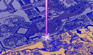
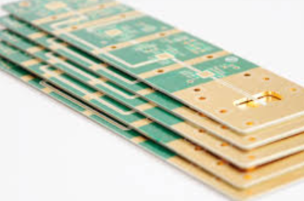
Fr4 multilayer pcb
Advantages Of Using FR4 Material In Multilayer PCBs
FR4 material has become a cornerstone in the design and manufacturing of multilayer printed circuit boards (PCBs), offering a range of advantages that make it a preferred choice for engineers and manufacturers alike. At the heart of its popularity is its excellent balance of performance, cost-effectiveness, and versatility, which collectively contribute to the efficient functioning of electronic devices across various industries.
One of the primary advantages of using FR4 material in multilayer PCBs is its outstanding electrical insulation properties.
FR4, a composite material made from woven fiberglass cloth with an epoxy resin binder, provides excellent dielectric strength. This characteristic is crucial in multilayer PCBs, where multiple layers of conductive pathways are stacked together. The insulating properties of FR4 ensure that there is minimal risk of electrical interference between these layers, thereby maintaining signal integrity and reducing the likelihood of short circuits.
In addition to its electrical insulation capabilities, FR4 material is renowned for its mechanical strength and durability.
It exhibits high tensile strength and resistance to mechanical stress, which is essential for maintaining the structural integrity of multilayer PCBs. This robustness allows FR4-based PCBs to withstand the rigors of manufacturing processes, such as drilling and soldering, as well as the operational stresses encountered in various applications. Consequently, devices that incorporate FR4 multilayer PCBs tend to have longer lifespans and greater reliability.
Moreover, FR4 material offers excellent thermal resistance, which is a critical factor in the performance of multilayer PCBs.
As electronic devices become more compact and powerful, they generate more heat, which can adversely affect their performance and longevity. FR4’s ability to withstand high temperatures without degrading ensures that multilayer PCBs can operate efficiently even in demanding thermal environments. This thermal stability is particularly beneficial in applications such as automotive electronics, aerospace systems, and industrial machinery, where temperature fluctuations are common.
Another significant advantage of FR4 material is its cost-effectiveness.
Compared to other high-performance materials used in PCB manufacturing, such as polyimide or ceramic substrates, FR4 is relatively inexpensive. This affordability makes it an attractive option for a wide range of applications, from consumer electronics to complex industrial systems. The cost savings associated with using FR4 do not come at the expense of quality or performance, making it a practical choice for both prototyping and mass production.
Furthermore, the versatility of FR4 material cannot be overstated.
It is compatible with a variety of PCB manufacturing processes and can be easily adapted to meet specific design requirements. Whether the application demands a simple two-layer board or a complex multilayer configuration, FR4 can be tailored to suit the needs of the project. This adaptability extends to the surface finish options available for FR4 PCBs, allowing for further customization based on the intended use and environmental conditions.
In conclusion, the advantages of using FR4 material in multilayer PCBs are manifold, encompassing electrical insulation, mechanical strength, thermal resistance, cost-effectiveness, and versatility. These attributes make FR4 an indispensable material in the electronics industry, supporting the development of reliable and efficient devices that meet the ever-evolving demands of modern technology. As the industry continues to advance, the role of FR4 in multilayer PCB design is likely to remain pivotal, ensuring that electronic devices can perform optimally in a wide array of applications.
Design Considerations For FR4 Multilayer PCBs
When designing FR4 multilayer printed circuit boards (PCBs), several critical considerations must be taken into account to ensure optimal performance and reliability.
FR4, a widely used material in PCB fabrication, is favored for its excellent balance of cost, mechanical strength, and electrical insulation properties. However, the complexity of multilayer PCBs necessitates a thorough understanding of various design elements to fully leverage the advantages of FR4.
To begin with, the number of layers in a multilayer PCB is a fundamental consideration.
The decision on the number of layers is influenced by the complexity of the circuit, the need for signal integrity, and the space constraints of the final product. More layers allow for greater routing flexibility and can help in minimizing electromagnetic interference (EMI) by providing dedicated ground and power planes. However, increasing the number of layers also raises manufacturing costs and can complicate the fabrication process. Therefore, a balance must be struck between performance requirements and budgetary constraints.
Another crucial aspect is the stack-up configuration, which refers to the arrangement of conductive and insulating layers within the PCB.
A well-designed stack-up can significantly enhance signal integrity and reduce EMI. Typically, a symmetrical stack-up is preferred to prevent warping during the manufacturing process. The placement of power and ground planes is also vital; they should be positioned to minimize loop areas and provide a low-impedance path for return currents. This configuration not only improves signal quality but also aids in thermal management by distributing heat more evenly across the board.
Material selection is another key consideration in the design of FR4 multilayer PCBs
. While FR4 is the standard choice due to its versatility, different grades of FR4 offer varying thermal and electrical properties. Designers must select a grade that aligns with the specific requirements of their application, such as operating temperature range and dielectric constant. Additionally, the thickness of the FR4 material can impact the board’s mechanical stability and impedance characteristics, necessitating careful selection based on the intended use case.
Signal integrity is a paramount concern in multilayer PCB design, particularly for high-speed applications.
To mitigate issues such as crosstalk and signal reflection, designers must pay close attention to trace width, spacing, and routing paths. Controlled impedance routing is often employed to ensure consistent signal transmission, which involves calculating the appropriate trace dimensions based on the dielectric properties of the FR4 material and the desired impedance value. Furthermore, the use of differential pairs and proper termination techniques can help maintain signal integrity across the board.
Thermal management is another critical factor, especially in densely packed multilayer PCBs.
The thermal conductivity of FR4 is relatively low, which can lead to heat buildup and potential failure if not addressed. Designers can incorporate thermal vias, heat sinks, and copper pours to enhance heat dissipation. Additionally, careful component placement and the use of thermal simulation tools can aid in identifying and mitigating potential hotspots.
In conclusion, designing FR4 multilayer PCBs requires a comprehensive approach that considers layer count, stack-up configuration, material selection, signal integrity, and thermal management. By carefully addressing these factors, designers can create PCBs that meet the demanding requirements of modern electronic applications while maintaining cost-effectiveness and reliability. The intricate interplay of these considerations underscores the importance of a meticulous design process in achieving successful outcomes in multilayer PCB projects.
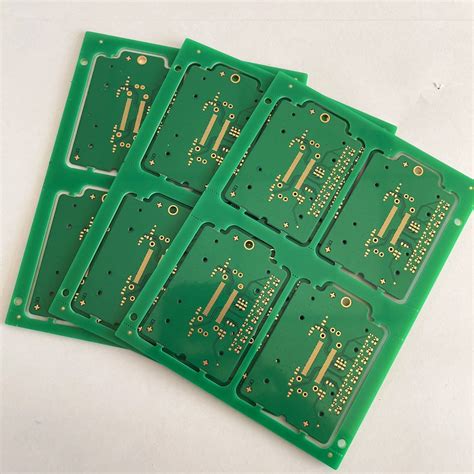
Manufacturing Process Of FR4 Multilayer PCBs
The manufacturing process of FR4 multilayer printed circuit boards (PCBs) is a complex and intricate procedure that requires precision and expertise. FR4, a composite material made from woven fiberglass cloth with an epoxy resin binder, is widely used in the electronics industry due to its excellent mechanical strength and electrical insulation properties. The process begins with the design phase, where engineers create a detailed schematic of the circuit, specifying the number of layers and the layout of components. This design is then translated into a digital format, which serves as a blueprint for the subsequent manufacturing stages.
Once the design is finalized, the production process commences with the preparation of the individual layers.
Each layer consists of a thin sheet of copper laminated onto the FR4 substrate. The copper is then coated with a photosensitive film, which is exposed to ultraviolet light through a photomask that corresponds to the circuit design. This exposure hardens the film in the areas where the copper is to remain, while the unexposed areas are subsequently removed using a chemical solution. This etching process reveals the desired copper traces that form the electrical pathways on each layer.
Following the etching process, the layers are aligned and stacked in the correct sequence.
This alignment is crucial, as any misalignment can lead to circuit failure. The stack is then subjected to a lamination process, where heat and pressure are applied to bond the layers together, forming a single, cohesive unit. This step is critical in ensuring the structural integrity and reliability of the multilayer PCB.
After lamination, the board undergoes drilling to create vias, which are small holes that allow electrical connections between the different layers.
These vias are plated with copper to ensure conductivity. The drilling process must be precise, as any deviation can compromise the functionality of the PCB. Once the vias are plated, the board is subjected to a series of inspections and tests to verify its electrical performance and structural integrity.
The next stage involves the application of a solder mask, which is a protective layer that prevents solder
from bridging between conductive traces and causing short circuits. The solder mask is typically green, although other colors are available. It is applied using a screen-printing process and then cured under ultraviolet light. Following this, a silkscreen layer is added to print component labels and other necessary markings on the board.
Finally, the board undergoes surface finishing, which involves coating the exposed copper areas with a protective layer to prevent oxidation and enhance solderability.
Common finishes include HASL (Hot Air Solder Leveling), ENIG (Electroless Nickel Immersion Gold), and OSP (Organic Solderability Preservative). Each finish has its advantages and is selected based on the specific requirements of the application.
In conclusion, the manufacturing process of FR4 multilayer PCBs is a meticulous and highly technical endeavor that demands precision at every stage. From design to final inspection, each step is critical in ensuring the production of reliable and high-performance PCBs. As technology continues to advance, the demand for multilayer PCBs is expected to grow, further underscoring the importance of mastering this complex manufacturing process.

Common Applications Of FR4 Multilayer PCBs
FR4 multilayer printed circuit boards (PCBs) have become a cornerstone in modern electronics, offering a versatile and reliable solution for a wide range of applications. These PCBs are constructed using multiple layers of FR4 material, a composite made from woven fiberglass cloth with an epoxy resin binder that is flame resistant. The inherent properties of FR4, such as its excellent mechanical strength, electrical insulation, and thermal stability, make it an ideal substrate for multilayer PCBs. As technology continues to advance, the demand for more complex and compact electronic devices has led to the widespread adoption of FR4 multilayer PCBs across various industries.
One of the most common applications of FR4 multilayer PCBs is in the telecommunications sector.
With the rapid expansion of communication networks and the increasing need for high-speed data transmission, these PCBs are essential in the development of routers, switches, and other networking equipment. The multilayer design allows for the integration of numerous circuits within a compact space, facilitating the efficient handling of complex signal processing tasks. Moreover, the reliability and durability of FR4 material ensure that these devices can withstand the rigors of continuous operation, making them indispensable in maintaining robust communication infrastructures.
In addition to telecommunications, the consumer electronics industry heavily relies on FR4 multilayer PCBs.
From smartphones and tablets to laptops and wearable devices, these PCBs are integral to the functionality and performance of modern gadgets. The ability to incorporate multiple layers of circuitry enables manufacturers to design smaller, more powerful devices without compromising on performance. Furthermore, the thermal stability of FR4 material helps in managing heat dissipation, which is crucial for maintaining the longevity and efficiency of electronic components in compact devices.
The automotive industry also benefits significantly from the use of FR4 multilayer PCBs.
As vehicles become increasingly sophisticated with the integration of advanced electronic systems, such as infotainment systems, navigation units, and driver assistance technologies, the need for reliable and efficient PCBs has grown. FR4 multilayer PCBs provide the necessary support for these complex systems, ensuring seamless operation and enhancing the overall driving experience. Additionally, the robustness of FR4 material makes it suitable for withstanding the harsh environmental conditions often encountered in automotive applications, such as extreme temperatures and vibrations.
Moreover, the aerospace and defense sectors have found FR4 multilayer PCBs to be invaluable in the development of cutting-edge technologies.
In these industries, where precision and reliability are paramount, the use of high-quality PCBs is critical. FR4 multilayer PCBs are employed in a variety of applications, including avionics systems, radar equipment, and communication devices. The ability to support high-density interconnections and complex circuitry makes them ideal for meeting the stringent requirements of aerospace and defense applications.
In conclusion, the versatility and reliability of FR4 multilayer PCBs have made them a preferred choice across numerous industries. Their ability to support complex circuitry within a compact form factor, coupled with the inherent properties of FR4 material, ensures their continued relevance in the face of evolving technological demands. As industries continue to push the boundaries of innovation, the role of FR4 multilayer PCBs in enabling advanced electronic solutions remains indispensable, underscoring their significance in the modern technological landscape.