From Design to Operation: A Comprehensive Guide to RF PCB Development
Introduction
Radio Frequency (RF) Printed Circuit Boards (PCBs) are essential components in modern wireless communication systems, including smartphones, Wi-Fi routers, satellite communications, and radar systems. Designing and operating an RF PCB requires specialized knowledge due to the high-frequency signals involved, which introduce challenges such as signal integrity, impedance matching, and electromagnetic interference (EMI). This article provides a detailed guide on the entire process—from RF PCB design considerations to fabrication, testing, and operation.
1. RF PCB Design Considerations
1.1 Material Selection
The choice of substrate material is critical in RF PCB design. Unlike standard FR4, RF PCBs often require low-loss dielectric materials such as:
- Rogers (RO4000 series) – Low dielectric loss, stable performance at high frequencies.
- Teflon (PTFE) – Excellent high-frequency properties but harder to manufacture.
- Ceramic-filled PTFE – Balances performance and manufacturability.
Key parameters to consider:
- Dielectric Constant (Dk) – Affects signal propagation speed.
- Dissipation Factor (Df) – Determines signal loss.
- Thermal Stability – Ensures consistent performance under temperature variations.
1.2 Transmission Line Design
RF signals require controlled impedance transmission lines to minimize reflections. Common types include:
- Microstrip – A trace over a ground plane, suitable for frequencies up to ~30 GHz.
- Stripline – A trace sandwiched between two ground planes, offering better EMI shielding.
- Coplanar Waveguide (CPW) – A trace with adjacent ground planes, useful for high-frequency applications.
Impedance matching (typically 50Ω or 75Ω) is crucial to prevent signal reflections. Tools like ADS (Advanced Design System) or ANSYS HFSS help simulate and optimize these structures.
1.3 Layout and Routing Best Practices
- Minimize Trace Lengths – Shorter traces reduce signal loss and phase distortion.
- Avoid Sharp Angles – Use curved or 45° bends to prevent impedance discontinuities.
- Ground Plane Integrity – Ensure a continuous ground plane beneath RF traces to reduce EMI.
- Component Placement – Keep RF components close to minimize parasitic effects.
1.4 Shielding and EMI Mitigation
- Use Ground Vias (Stitching Vias) – Prevent cavity resonances and reduce radiation.
- Faraday Cages – Metallic enclosures to block external interference.
- Differential Signaling – Reduces noise susceptibility in high-speed RF circuits.
2. Fabrication and Manufacturing Challenge
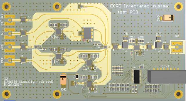
2.1 PCB Stackup Design
A well-planned stackup ensures signal integrity and manufacturability. Considerations include:
- Layer Arrangement – RF signals should be on outer layers to minimize via transitions.
- Controlled Impedance Layers – Requires precise dielectric thickness and trace width control.
2.2 Manufacturing Tolerances
RF PCBs demand tighter tolerances than standard boards:
- Trace Width & Spacing – ±10% variation can affect impedance.
- Dielectric Thickness – Must be consistent to maintain Dk.
- Surface Finish – ENIG (Electroless Nickel Immersion Gold) is preferred for RF due to its smooth surface and oxidation resistance.
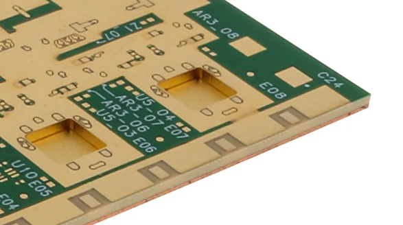
2.3 Via Design
- Blind/Buried Vias – Used to minimize stub effects in high-frequency designs.
- Via Filling – Conductive or non-conductive fill to improve signal integrity.
3. Testing and Validation
3.1 Vector Network Analyzer (VNA) Testing
A VNA measures S-parameters (S11, S21) to evaluate:
- Return Loss (S11) – Indicates impedance matching.
- Insertion Loss (S21) – Measures signal attenuation.
3.2 Time-Domain Reflectometry (TDR)
TDR identifies impedance mismatches and discontinuities along transmission lines.
3.3 Spectrum Analyzer Testing
Used to detect unwanted harmonics, spurious emissions, and noise in RF circuits.
3.4 Environmental Testing
- Thermal Cycling – Ensures stability across operating temperatures.
- Vibration Testing – Validates mechanical robustness.
4. Operational Consideration
4.1 Power Handling and Thermal Management
- Heat Dissipation – RF amplifiers and power circuits generate heat; use thermal vias and heatsinks.
- Current Handling – Wide traces and thick copper layers reduce resistive losses.
4.2 Signal Integrity in Real-World Conditions
- Antenna Coupling – Ensure minimal interference between RF and digital sections.
- Environmental Noise – Shielding and filtering mitigate external RFI (Radio Frequency Interference).
4.3 Firmware and Calibration
- Automatic Gain Control (AGC) – Adjusts signal levels dynamically.
- Digital Pre-Distortion (DPD) – Compensates for nonlinearities in RF power amplifiers.
5. Future Trends in RF PCB Technology
- 5G and mmWave PCBs – Require advanced materials (e.g., liquid crystal polymer).
- AI-Optimized RF Designs – Machine learning aids in automated impedance tuning.
- Integrated Antenna Arrays – On-PCB antennas for compact wireless systems.
Conclusion
Designing and operating an RF PCB involves a multidisciplinary approach, combining electromagnetic theory, material science, and precision manufacturing. By following best practices in layout, material selection, and testing, engineers can develop high-performance RF circuits that meet the demands of modern wireless systems. As technology advances, RF PCBs will continue to evolve, enabling faster, more reliable communication networks.