Fundamentals of Stitching Vias in PCB Design
1. Introduction to Stitching Vias
Printed Circuit Board (PCB) design involves numerous techniques to ensure signal integrity, electromagnetic compatibility (EMC), and mechanical stability. One such technique is the use of stitching vias, which are strategically placed vias that help in creating a low-impedance return path for high-frequency signals, reducing electromagnetic interference (EMI), and improving thermal dissipation.
Stitching vias are commonly used in multilayer PCBs, particularly in designs involving high-speed signals, RF circuits, and power distribution networks. This article explores the fundamentals of stitching vias, their purpose, design considerations, and best practices for implementation.
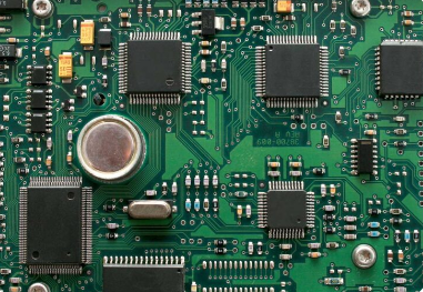
2. What Are Stitching Vias?
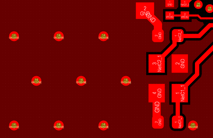
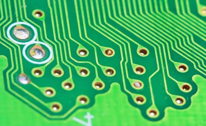
Stitching vias are small plated-through holes (PTH) that electrically connect different layers of a PCB, typically between ground or power planes. Unlike regular signal vias, which route signals between layers, stitching vias are primarily used to:
- Enhance ground/power plane connectivity – They reduce loop inductance by providing multiple return paths.
- Mitigate EMI – They help contain electromagnetic fields by creating a Faraday cage effect.
- Improve thermal conductivity – They aid in heat dissipation by connecting copper planes.
- Strengthen mechanical stability – They reinforce the PCB structure, especially in flexible or rigid-flex designs.
Stitching vias are often arranged in a grid or along the edges of critical signal traces to ensure optimal performance.
3. Why Are Stitching Vias Important?
3.1. Reducing Ground Loops and Impedance
High-speed signals require a low-impedance return path to minimize noise and signal distortion. Without proper stitching, return currents may take longer paths, increasing loop inductance and causing EMI issues. Stitching vias provide multiple parallel return paths, reducing overall impedance.
3.2. EMI Shielding and Crosstalk Reduction
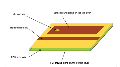
In RF and high-frequency designs, stitching vias create a “via fence” around sensitive traces or components, acting as a shield against external interference. This technique is crucial in preventing crosstalk between adjacent signal lines.
3.3. Thermal Management
Stitching vias help distribute heat more evenly across layers by connecting copper planes, which is particularly useful in high-power applications.
3.4. Structural Integrity
In flexible PCBs, stitching vias reinforce the board, preventing delamination and improving durability under mechanical stress.
4. Types of Stitching Vias
4.1. Ground Stitching Vias
These vias connect ground planes across different layers, ensuring a continuous return path for signals. They are commonly placed near high-speed traces and around PCB edges.
4.2. Power Stitching Vias
Used in power distribution networks (PDNs), these vias connect power planes to reduce IR drop and improve current flow.
4.3. Via Fences (Shielding Vias)
A row of stitching vias placed around high-frequency traces or components to block EMI and reduce radiation.
4.4. Thermal Stitching Vias
Designed to enhance heat dissipation, these vias connect copper pours and thermal pads to spread heat efficiently.
5. Design Considerations for Stitching Vias
5.1. Via Spacing and Placement
- Rule of Thumb: A typical stitching via spacing is λ/10 (where λ is the wavelength of the highest frequency signal).
- For most applications, a spacing of 100-200 mils (2.54-5.08 mm) is sufficient.
- In RF designs, tighter spacing (e.g., 50 mils or less) may be required.
5.2. Via Diameter and Aspect Ratio
- Drill diameter: Typically 8-12 mils (0.2-0.3 mm).
- Pad size: At least 4-6 mils larger than the drill diameter.
- Aspect ratio (depth/diameter): Should be ≤ 10:1 to ensure reliable plating.
5.3. Anti-Pad and Clearance
- Ensure proper clearance in non-connected layers to avoid unintended shorts.
- Anti-pads (isolated regions around vias in non-target layers) should be designed carefully.
5.4. Via Fill and Plugging
- Conductive epoxy fill: Used in high-reliability applications to improve thermal and electrical performance.
- Non-conductive fill: Used when mechanical stability is a priority.
6. Best Practices for Implementing Stitching Vias
- Use a Grid Pattern – Uniform distribution ensures consistent impedance and EMI shielding.
- Stitch Along PCB Edges – Helps contain radiated emissions.
- Avoid Stitching Under Components – May interfere with solder joints or cause thermal stress.
- Optimize for Manufacturing – Follow PCB fab guidelines to avoid drill breakage or plating issues.
- Simulate Before Finalizing – Use EM simulation tools (e.g., Ansys HFSS, CST) to verify effectiveness.
7. Common Mistakes to Avoid
- Insufficient Via Count – Too few vias increase impedance and degrade performance.
- Poor Placement – Randomly placed vias may not provide effective shielding.
- Ignoring Return Paths – Ensure stitching vias align with signal return currents.
- Overlooking Thermal Effects – Excessive vias in small areas can cause warping or delamination.
8. Conclusion
Stitching vias play a crucial role in modern PCB design, particularly in high-speed, RF, and high-power applications. By providing low-impedance return paths, reducing EMI, and improving thermal management, they enhance both electrical performance and structural integrity. Proper design and implementation require careful consideration of spacing, placement, and manufacturing constraints. Following industry best practices ensures optimal performance and reliability in complex PCB designs.
By mastering the use of stitching vias, engineers can significantly improve signal integrity, reduce noise, and create more robust electronic systems.