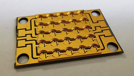
Ground layer pcb
Understanding Ground Layer Design in PCB Layout
In the realm of electronic design, the printed circuit board (PCB) serves as the backbone of most electronic devices, providing the necessary support and electrical connections for various components. Among the critical aspects of PCB design is the ground layer, which plays a pivotal role in ensuring the functionality and reliability of the circuit. Understanding the intricacies of ground layer design is essential for engineers and designers aiming to optimize their PCB layouts.
The ground layer in a PCB is a dedicated layer that serves as a common return path for electric current.
It is crucial for maintaining signal integrity, reducing electromagnetic interference (EMI), and ensuring the overall stability of the circuit. A well-designed ground layer can significantly enhance the performance of a PCB by minimizing noise and preventing potential issues that could arise from poor grounding practices. To achieve this, designers must consider several factors, including the layout, placement, and connection of the ground layer.
One of the primary considerations in ground layer design is the layout configuration.
Typically, a ground layer is implemented as a solid plane, which provides a low-impedance path for current flow. This configuration helps in reducing voltage drops and maintaining a consistent reference voltage across the PCB. Moreover, a solid ground plane acts as a shield against electromagnetic interference, thereby protecting sensitive components from external noise sources. In contrast, a fragmented or poorly connected ground layer can lead to increased impedance, resulting in signal degradation and potential circuit malfunctions.
In addition to the layout, the placement of the ground layer within the PCB stack-up is another critical factor.
Ideally, the ground layer should be positioned adjacent to the power layer to form a parallel plate capacitor, which helps in decoupling high-frequency noise. This arrangement not only enhances the power distribution network but also improves the overall electromagnetic compatibility (EMC) of the PCB. Furthermore, placing the ground layer close to signal layers can reduce the loop area, thereby minimizing inductive coupling and crosstalk between traces.
The connection of the ground layer to other components and layers is equally important.
Designers must ensure that the ground layer is properly connected to all relevant components, including connectors, mounting holes, and other layers. This can be achieved through the use of vias, which provide vertical connections between different layers of the PCB. It is essential to strategically place these vias to maintain a continuous ground path and avoid creating isolated ground islands, which can lead to potential grounding issues.
Moreover, the concept of ground separation is often employed in complex PCB designs to isolate different sections of the circuit.
This technique involves creating separate ground regions for analog and digital components to prevent noise coupling between them. However, care must be taken to ensure that these separate ground regions are properly connected at a single point, often referred to as a star ground, to maintain a common reference potential.
In conclusion, the design of the ground layer in a PCB layout is a critical aspect that requires careful consideration and planning. By understanding the principles of ground layer design, including layout configuration, placement, and connection, designers can create PCBs that are not only efficient and reliable but also resilient to noise and interference. As technology continues to advance, the importance of a well-designed ground layer will remain a fundamental aspect of successful PCB design.
Best Practices for Ground Layer Routing in PCBs
In the realm of printed circuit board (PCB) design, the ground layer plays a pivotal role in ensuring the overall functionality and reliability of electronic devices. As the foundation for electrical stability, the ground layer serves as a reference point for all voltage levels within the circuit, making its proper routing essential. To achieve optimal performance, designers must adhere to best practices that enhance the integrity of the ground layer, thereby minimizing potential issues such as electromagnetic interference (EMI) and signal integrity problems.
One of the foremost considerations in ground layer routing is the establishment of a continuous ground plane.
A solid ground plane provides a low-impedance path for return currents, which is crucial for maintaining signal integrity. By minimizing the impedance, designers can reduce the potential for voltage drops and noise, which can adversely affect the performance of the circuit. To this end, it is advisable to avoid splitting the ground plane unnecessarily, as discontinuities can lead to increased loop areas and, consequently, higher EMI emissions.
Moreover, the placement of vias is another critical aspect of ground layer routing.
Vias, which are used to connect different layers of a PCB, should be strategically placed to ensure efficient current flow. It is recommended to use multiple vias to connect the ground plane to other layers, thereby reducing inductance and improving the overall grounding performance. Additionally, designers should be cautious about placing vias too close to signal traces, as this can introduce unwanted coupling and degrade signal quality.
Transitioning to the topic of component placement, it is essential to position components in a manner that facilitates effective grounding.
Components that are sensitive to noise, such as analog and digital circuits, should be placed close to the ground plane to minimize the length of return paths. This proximity helps in reducing the loop area, which is a significant factor in controlling EMI. Furthermore, separating analog and digital ground planes can be beneficial in preventing noise from digital circuits from affecting sensitive analog components. However, care must be taken to connect these planes at a single point to avoid ground loops.
In addition to component placement, the routing of traces also plays a significant role in ground layer design.
Traces should be routed in a way that minimizes their length and avoids crossing over splits in the ground plane. When traces must cross a split, it is advisable to use a bridge capacitor to provide a low-impedance path for high-frequency signals. This practice helps in maintaining signal integrity and reducing potential interference.
Furthermore, the use of decoupling capacitors is a well-established practice in enhancing the performance of the ground layer.
These capacitors should be placed as close as possible to the power pins of integrated circuits to provide a local energy reservoir. By doing so, they help in stabilizing the power supply and reducing voltage fluctuations, which can otherwise propagate through the ground plane and affect other components.
In conclusion, the effective routing of the ground layer in PCBs is a critical aspect of circuit design that requires careful consideration and adherence to best practices. By ensuring a continuous ground plane, strategic placement of vias, thoughtful component positioning, and proper trace routing, designers can significantly enhance the performance and reliability of their electronic devices. These practices, coupled with the use of decoupling capacitors, contribute to a robust grounding strategy that mitigates potential issues and ensures the seamless operation of the circuit.
The Role of Ground Layers in Signal Integrity for PCBs
In the realm of printed circuit board (PCB) design, the ground layer plays a pivotal role in ensuring signal integrity, a critical aspect that directly influences the performance and reliability of electronic devices. As electronic systems become increasingly complex, with higher speeds and greater functionality, maintaining signal integrity has become a paramount concern for engineers and designers. The ground layer, often referred to as the ground plane, serves as a fundamental component in achieving this goal.
To begin with, the ground layer acts as a reference point for all voltage levels within the circuit.
This is essential for the proper functioning of electronic components, as it ensures that signals are accurately interpreted by the receiving devices. Without a stable reference, signals can become distorted, leading to errors and malfunctions. Moreover, the ground layer helps to minimize electromagnetic interference (EMI), which can be a significant source of signal degradation. By providing a low-impedance path for return currents, the ground layer effectively reduces the loop area through which electromagnetic fields can couple, thereby mitigating the impact of EMI on signal integrity.
In addition to its role in reducing EMI, the ground layer also plays a crucial part in controlling crosstalk between adjacent signal traces.
Crosstalk occurs when a signal transmitted on one trace induces an unwanted signal on a neighboring trace, potentially leading to data corruption. The ground layer helps to shield signal traces from one another, thereby minimizing the potential for crosstalk. This is particularly important in high-speed digital circuits, where even minor crosstalk can result in significant performance issues.
Furthermore, the ground layer contributes to the overall thermal management of the PCB.
As electronic components operate, they generate heat, which must be effectively dissipated to prevent overheating and ensure reliable operation. The ground layer, being a large copper plane, acts as a heat sink, spreading the heat generated by components across a larger area and facilitating its dissipation. This not only helps to maintain signal integrity by preventing thermal-induced variations in electrical characteristics but also extends the lifespan of the components.
Another critical aspect of the ground layer is its role in power distribution.
In many PCB designs, the ground layer is used in conjunction with power planes to form a power distribution network. This network ensures that all components receive a stable and consistent power supply, which is essential for maintaining signal integrity. Variations in power supply can lead to fluctuations in signal levels, resulting in errors and reduced performance. By providing a robust power distribution network, the ground layer helps to prevent such issues.
In conclusion, the ground layer is an indispensable element in the design of PCBs, playing a multifaceted role in ensuring signal integrity. From providing a stable reference point and reducing electromagnetic interference to minimizing crosstalk and aiding in thermal management, the ground layer is integral to the reliable operation of electronic devices. As technology continues to advance, the importance of the ground layer in maintaining signal integrity will only grow, underscoring the need for careful consideration and implementation in PCB design. Through its various functions, the ground layer not only enhances the performance of electronic systems but also contributes to their longevity and dependability.

Common Mistakes to Avoid in Ground Layer PCB Design
In the realm of printed circuit board (PCB) design, the ground layer plays a pivotal role in ensuring the functionality and reliability of electronic devices. However, designing an effective ground layer is fraught with potential pitfalls that can compromise the performance of the entire system. Understanding and avoiding these common mistakes is crucial for engineers and designers aiming to optimize their PCB designs.
One prevalent mistake in ground layer PCB design is the improper allocation of ground planes.
A ground plane serves as a reference point for all signals and provides a return path for current. When designers fail to allocate sufficient space for the ground plane, it can lead to increased electromagnetic interference (EMI) and signal integrity issues. To mitigate this, it is essential to dedicate an entire layer to the ground plane whenever possible, ensuring that it is continuous and uninterrupted. This approach minimizes impedance and enhances the overall performance of the PCB.
Another common error is neglecting the importance of via placement.
Vias, which are used to connect different layers of a PCB, can introduce inductance and resistance if not placed strategically. Poorly placed vias can disrupt the current return path, leading to increased noise and potential signal distortion. To avoid this, designers should place vias close to the components they serve, ensuring a direct and efficient path for current flow. Additionally, using multiple vias in parallel can help reduce inductance and improve the reliability of the ground connection.
Furthermore, designers often overlook the significance of maintaining a low-impedance path for the ground layer.
High impedance in the ground path can result in voltage drops and ground loops, which can severely affect the performance of the PCB. To address this, it is advisable to use wide traces and planes for the ground layer, minimizing resistance and ensuring a stable reference point for all signals. Additionally, designers should avoid splitting the ground plane, as this can create isolated sections that disrupt the current flow and increase impedance.
In addition to these technical considerations, it is crucial to pay attention to the placement of decoupling capacitors.
These components are essential for filtering out noise and stabilizing the power supply to integrated circuits. A common mistake is placing decoupling capacitors too far from the power pins of the components they serve. This can lead to increased inductance and reduced effectiveness in noise suppression. To optimize their performance, decoupling capacitors should be placed as close as possible to the power pins, with a direct and short connection to the ground plane.
Moreover, designers should be cautious about the potential for ground loops, which occur when there are multiple paths for current to return to the ground.
Ground loops can introduce unwanted noise and interfere with signal integrity. To prevent this, it is important to establish a single, continuous ground path and avoid creating closed loops in the design. This can be achieved by carefully planning the layout and ensuring that all components share a common ground reference.
In conclusion, designing an effective ground layer in a PCB requires careful consideration of various factors, including ground plane allocation, via placement, impedance management, decoupling capacitor placement, and ground loop prevention. By avoiding these common mistakes, designers can enhance the performance and reliability of their PCBs, ultimately leading to more efficient and robust electronic devices. Through meticulous planning and attention to detail, the challenges associated with ground layer PCB design can be successfully navigated, resulting in superior outcomes for both designers and end-users alike.