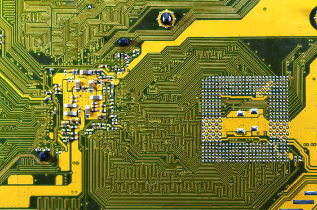
Hdi pcb material
Advantages Of Using HDI PCB Material In Modern Electronics
High-Density Interconnect (HDI) printed circuit boards (PCBs) have become a cornerstone in the advancement of modern electronics, offering a multitude of advantages that cater to the ever-evolving demands of the industry.
One of the primary benefits of using HDI PCB material is its ability to support miniaturization.
As electronic devices become increasingly compact, the need for smaller, yet more powerful, components has surged. HDI PCBs facilitate this trend by allowing for a higher density of components on a single board, thereby enabling the production of smaller devices without compromising on functionality.
In addition to supporting miniaturization, HDI PCBs enhance electrical performance.
The reduced distance between components on an HDI board minimizes signal loss and electromagnetic interference, leading to improved signal integrity. This is particularly crucial in high-speed applications where even minor signal degradation can result in significant performance issues. Consequently, HDI PCBs are often the preferred choice for applications requiring high-speed data transmission, such as telecommunications and advanced computing systems.
Moreover, the use of HDI PCB material contributes to increased reliability and durability.
The advanced manufacturing processes involved in producing HDI boards, such as laser drilling and sequential lamination, result in more robust and precise interconnections. These processes reduce the likelihood of defects and improve the overall mechanical strength of the board. As a result, devices utilizing HDI PCBs tend to exhibit longer lifespans and greater resistance to environmental stressors, making them ideal for use in critical applications like medical devices and aerospace technology.
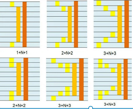
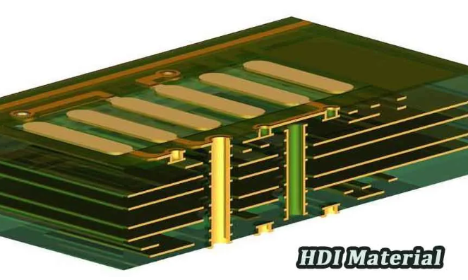
Another significant advantage of HDI PCBs is their ability to support higher layer counts without a corresponding increase in board thickness.
Traditional PCBs often become unwieldy and difficult to manage as the number of layers increases. In contrast, HDI technology allows for the integration of multiple layers within a compact form factor, facilitating the design of complex circuits in a more efficient manner. This capability is particularly beneficial in the development of sophisticated electronic systems, where space constraints and performance requirements necessitate intricate multi-layer designs.
Furthermore, HDI PCBs offer enhanced thermal management capabilities.
The high component density and advanced materials used in HDI boards contribute to more effective heat dissipation, which is essential for maintaining optimal performance and preventing overheating. This is especially important in high-power applications, such as power electronics and automotive systems, where efficient thermal management is critical to ensuring the reliability and safety of the device.
In addition to these technical advantages, the use of HDI PCB material can also lead to cost savings in the long run.
While the initial manufacturing costs of HDI boards may be higher compared to traditional PCBs, the benefits of improved performance, reliability, and miniaturization often result in lower overall costs. For instance, the reduced need for additional components and connectors, as well as the potential for fewer assembly steps, can lead to significant savings in production and maintenance expenses.
In conclusion, the advantages of using HDI PCB material in modern electronics are manifold. From supporting miniaturization and enhancing electrical performance to increasing reliability and enabling complex multi-layer designs, HDI PCBs address many of the challenges faced by today’s electronic designers. As technology continues to advance, the role of HDI PCBs in driving innovation and improving the functionality of electronic devices is likely to become even more pronounced, solidifying their position as a critical component in the future of electronics.
Comparing HDI PCB Material To Traditional PCB Substrates
High-Density Interconnect (HDI) printed circuit boards (PCBs) have revolutionized the electronics industry by enabling more compact, efficient, and high-performance devices. When comparing HDI PCB materials to traditional PCB substrates, several key differences emerge that highlight the advantages and specific applications of each. Understanding these distinctions is crucial for engineers and designers aiming to optimize their electronic products.
To begin with, HDI PCBs utilize advanced materials and manufacturing techniques that allow for a higher density of components and interconnections.
This is achieved through the use of microvias, finer lines, and smaller pads, which are not typically feasible with traditional PCB substrates. Traditional PCBs, often made from materials like FR-4, have limitations in terms of layer count and component density due to their relatively larger via sizes and thicker traces. In contrast, HDI PCBs employ materials such as modified epoxy resins, polyimides, and other high-performance laminates that support the intricate designs required for modern electronics.
One of the primary benefits of HDI PCB materials is their ability to support higher signal integrity and faster signal transmission.
The advanced materials used in HDI PCBs have lower dielectric constants and dissipation factors, which reduce signal loss and crosstalk. This is particularly important in high-frequency applications where maintaining signal integrity is critical. Traditional PCB substrates, while adequate for many applications, often struggle to meet the stringent requirements of high-speed and high-frequency circuits due to their higher dielectric losses.
Moreover, the thermal performance of HDI PCB materials is superior to that of traditional substrates.
The materials used in HDI PCBs typically have better thermal conductivity and can withstand higher temperatures, making them suitable for applications that generate significant heat. This is a crucial consideration in the design of compact electronic devices, where efficient heat dissipation is necessary to ensure reliability and longevity. Traditional PCB materials, such as standard FR-4, may not offer the same level of thermal management, potentially leading to overheating and reduced performance in demanding applications.
Another significant advantage of HDI PCB materials is their contribution to miniaturization.
As consumer electronics continue to shrink in size while increasing in functionality, the need for smaller, more efficient PCBs becomes paramount. HDI technology allows for the integration of more components in a smaller footprint, enabling the development of sleek, lightweight devices without compromising performance. Traditional PCB substrates, with their larger vias and traces, are less suited to such compact designs, often resulting in bulkier and less efficient products.
Furthermore, the reliability and durability of HDI PCBs are enhanced by the use of advanced materials and manufacturing processes.
The precision and accuracy required in HDI fabrication lead to fewer defects and higher overall quality. This is particularly beneficial in applications where reliability is critical, such as in medical devices, aerospace, and automotive electronics. Traditional PCBs, while reliable in many contexts, may not offer the same level of performance in these high-stakes environments.
In conclusion, the comparison between HDI PCB materials and traditional PCB substrates reveals several distinct advantages of HDI technology. From improved signal integrity and thermal performance to enhanced miniaturization and reliability, HDI PCBs offer significant benefits for modern electronic applications. As technology continues to advance, the adoption of HDI materials is likely to increase, driving further innovation and efficiency in the electronics industry.
Key Properties Of HDI PCB Material For High-Performance Applications
High-Density Interconnect (HDI) printed circuit boards (PCBs) have become a cornerstone in the development of advanced electronic devices, primarily due to their ability to support higher wiring density and more complex circuitry. The key properties of HDI PCB material are crucial for ensuring high performance in various applications, ranging from consumer electronics to aerospace systems. Understanding these properties is essential for engineers and designers who aim to leverage the full potential of HDI technology.
One of the most significant properties of HDI PCB material is its dielectric constant (Dk).
The dielectric constant measures the material’s ability to store electrical energy in an electric field. A lower dielectric constant is generally preferred for high-frequency applications because it reduces signal loss and enhances signal integrity. Materials with a low Dk, such as certain types of advanced laminates, are often chosen for HDI PCBs to ensure minimal signal degradation and optimal performance.
In addition to the dielectric constant, the dissipation factor (Df) is another critical property.
The dissipation factor quantifies the energy loss in the dielectric material as heat. A lower dissipation factor indicates that the material is more efficient at transmitting signals with minimal energy loss. This property is particularly important in high-speed and high-frequency applications, where even small losses can significantly impact overall performance. Therefore, selecting HDI PCB materials with a low dissipation factor is essential for maintaining signal integrity and achieving high performance.
Thermal management is another vital aspect of HDI PCB material properties.
As electronic devices become more compact and powerful, the ability to dissipate heat effectively becomes increasingly important. HDI PCBs often incorporate materials with high thermal conductivity to facilitate efficient heat dissipation. This helps prevent overheating and ensures the reliability and longevity of the electronic components. Materials such as copper-clad laminates and thermally conductive prepregs are commonly used in HDI PCBs to enhance thermal performance.
Mechanical properties, including tensile strength and flexibility, also play a crucial role in the performance of HDI PCBs.
The material must be robust enough to withstand the mechanical stresses encountered during manufacturing and operation. At the same time, it should offer sufficient flexibility to accommodate the intricate designs and fine features characteristic of HDI technology. Advanced composite materials and specialized resins are often employed to achieve the desired balance of strength and flexibility in HDI PCBs.
Furthermore, the coefficient of thermal expansion (CTE) is a key property that affects the reliability of HDI PCBs.
The CTE measures how much a material expands or contracts with changes in temperature. A mismatch in CTE between the PCB material and the components can lead to mechanical stress and potential failure. Therefore, selecting materials with a CTE that closely matches that of the components is essential for ensuring the long-term reliability of HDI PCBs.
Lastly, the environmental stability of HDI PCB materials cannot be overlooked.
These materials must be resistant to moisture, chemicals, and other environmental factors that could degrade their performance over time. High-quality HDI PCB materials are designed to withstand harsh conditions, ensuring consistent performance in a wide range of applications.
In conclusion, the key properties of HDI PCB material, including dielectric constant, dissipation factor, thermal management, mechanical properties, coefficient of thermal expansion, and environmental stability, are critical for achieving high performance in advanced electronic applications. By carefully selecting materials that meet these criteria, engineers and designers can ensure the reliability, efficiency, and longevity of their HDI PCBs, ultimately contributing to the success of their high-performance applications.
Innovations In HDI PCB Material For Next-Generation Devices
High-Density Interconnect (HDI) printed circuit boards (PCBs) have become a cornerstone in the development of next-generation electronic devices. As the demand for more compact, efficient, and powerful gadgets continues to rise, innovations in HDI PCB materials are playing a crucial role in meeting these requirements. The evolution of these materials is not only enhancing the performance of electronic devices but also pushing the boundaries of what is technologically possible.
One of the primary drivers behind the advancements in HDI PCB materials is the need for miniaturization.
Modern electronic devices, from smartphones to wearable technology, require increasingly smaller and more complex PCBs. Traditional materials, such as FR4, are often insufficient for these applications due to their limitations in supporting high-density designs. Consequently, new materials with superior properties are being developed to address these challenges. For instance, materials like polyimide and liquid crystal polymer (LCP) offer excellent thermal stability and mechanical flexibility, making them ideal for use in HDI PCBs.
In addition to miniaturization, the performance of electronic devices is heavily influenced by the electrical properties of the PCB materials.
Innovations in this area have led to the development of materials with lower dielectric constants and dissipation factors. These properties are essential for high-speed signal transmission, which is critical in applications such as 5G communication and advanced computing. By reducing signal loss and interference, these advanced materials ensure that devices can operate at higher speeds and with greater reliability.
Thermal management is another critical aspect that has driven innovations in HDI PCB materials.
As electronic devices become more powerful, they generate more heat, which can adversely affect their performance and longevity. Advanced materials with high thermal conductivity, such as metal-core PCBs and ceramic-filled laminates, are being increasingly utilized to dissipate heat more effectively. These materials help maintain optimal operating temperatures, thereby enhancing the overall performance and durability of the devices.
Moreover, the environmental impact of electronic devices is an important consideration in the development of new HDI PCB materials.
There is a growing emphasis on sustainability and the use of eco-friendly materials in the electronics industry. Innovations in this area include the development of halogen-free laminates and the use of bio-based resins. These materials not only reduce the environmental footprint of electronic devices but also comply with stringent regulatory standards, making them a preferred choice for manufacturers.
The integration of advanced materials in HDI PCBs also facilitates the incorporation of additional functionalities into electronic devices.
For example, the use of flexible and stretchable materials enables the creation of bendable and wearable electronics. These innovations open up new possibilities for device design and application, ranging from medical devices to consumer electronics. The ability to integrate sensors, antennas, and other components directly into the PCB further enhances the functionality and versatility of next-generation devices.
In conclusion, the continuous advancements in HDI PCB materials are pivotal in driving the evolution of next-generation electronic devices. By addressing the challenges of miniaturization, improving electrical and thermal performance, promoting sustainability, and enabling new functionalities, these innovations are setting the stage for a new era of technological progress. As research and development in this field continue to advance, we can expect even more groundbreaking materials to emerge, further pushing the limits of what is possible in electronic device design and performance.