Hdi pcb process flow
Understanding The Basics Of HDI PCB Design And Manufacturing
High-Density Interconnect (HDI) printed circuit boards (PCBs) represent a significant advancement in the field of electronics, offering enhanced performance and miniaturization capabilities. Understanding the basics of HDI PCB design and manufacturing is crucial for engineers and designers aiming to leverage these benefits in modern electronic devices. The HDI PCB process flow involves several intricate steps, each contributing to the overall functionality and reliability of the final product.
To begin with, HDI PCBs are characterized by their higher wiring density per unit area compared to traditional PCBs.
This is achieved through the use of finer lines and spaces, smaller vias, and capture pads, as well as higher connection pad density. The process starts with the design phase, where engineers utilize advanced software tools to create detailed schematics and layouts. This stage is critical, as it sets the foundation for the entire manufacturing process. Designers must consider various factors such as signal integrity, thermal management, and mechanical constraints to ensure optimal performance.
Following the design phase, the manufacturing process commences with the selection of appropriate materials.
HDI PCBs typically use high-performance laminates and substrates that can withstand the rigors of advanced applications. The choice of materials impacts not only the electrical properties but also the thermal and mechanical characteristics of the PCB. Once the materials are selected, the next step involves the creation of the PCB layers. This is achieved through a process called lamination, where multiple layers of dielectric material are bonded together under heat and pressure.
Subsequently, the focus shifts to the drilling process, which is a defining feature of HDI technology.
Unlike conventional PCBs, HDI boards utilize microvias, which are significantly smaller and allow for more compact designs. These microvias are typically laser-drilled, offering precision and accuracy that mechanical drilling cannot achieve. The use of microvias enables designers to place components closer together, reducing the overall size of the PCB while maintaining or even enhancing its functionality.
After drilling, the next step is the metallization process, where the drilled holes are plated with a conductive material, usually copper.
This step is crucial for establishing electrical connections between different layers of the PCB. The plating process must be meticulously controlled to ensure uniformity and reliability of the connections. Following metallization, the PCB undergoes a series of etching processes to define the circuit patterns. This involves removing excess copper to create the desired traces and pads, which form the electrical pathways on the board.
As the manufacturing process progresses, the PCB is subjected to various testing and inspection procedures to ensure compliance with design specifications and quality standards.
These tests include electrical testing, where the board is checked for continuity and isolation, as well as visual inspections to identify any physical defects. The final stages of the HDI PCB process flow involve surface finishing and assembly. Surface finishes such as ENIG (Electroless Nickel Immersion Gold) or HASL (Hot Air Solder Leveling) are applied to protect the copper surfaces and enhance solderability.
In conclusion, the HDI PCB process flow is a complex and meticulous sequence of steps that demands precision and expertise. From design to assembly, each phase plays a vital role in ensuring the performance and reliability of the final product. As electronic devices continue to evolve, the demand for HDI PCBs is expected to grow, underscoring the importance of understanding their design and manufacturing processes.
Key Steps In The HDI PCB Fabrication Process
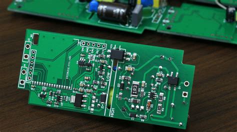
The fabrication of High-Density Interconnect (HDI) printed circuit boards (PCBs) is a sophisticated process that involves several critical steps, each contributing to the overall functionality and reliability of the final product. As electronic devices continue to shrink in size while increasing in complexity, HDI PCBs have become essential due to their ability to support higher wiring density and finer lines and spaces. Understanding the key steps in the HDI PCB fabrication process is crucial for anyone involved in electronics manufacturing or design.
The process begins with the design phase, where engineers use advanced software tools to create a detailed layout of the PCB.
This layout includes the placement of components, the routing of electrical connections, and the specification of layer stack-ups. The design must account for the unique requirements of HDI technology, such as microvias and fine lines, which allow for more compact and efficient circuit designs. Once the design is finalized, it is converted into a format suitable for manufacturing, typically a Gerber file.
Following the design phase, the next step is the selection of materials.
HDI PCBs often require specialized materials that can withstand the demands of high-density applications. These materials include high-performance laminates and prepregs that offer superior thermal and electrical properties. The choice of materials is critical, as it impacts the board’s performance, reliability, and cost.
Once the materials are selected, the fabrication process moves to the creation of the inner layers.
This involves laminating the chosen materials together and then etching the circuit patterns onto these layers. The etching process is precise, ensuring that the intricate designs are accurately transferred onto the board. After etching, the layers are inspected for defects, as any imperfections at this stage can compromise the entire board.
The next critical step is the drilling of vias, which are small holes that allow electrical connections between different layers of the PCB.
In HDI PCBs, microvias are commonly used due to their smaller size and ability to support higher densities. These microvias are typically created using laser drilling, which offers the precision required for such small features. After drilling, the vias are plated with copper to ensure reliable electrical connections.
Subsequently, the outer layers of the PCB are fabricated.
This involves a similar process of laminating, etching, and plating as used for the inner layers. However, additional care is taken to ensure that the outer layers align perfectly with the inner layers, as any misalignment can lead to functional issues. Once the outer layers are completed, the entire board undergoes a series of inspections and tests to verify its integrity and performance.
Finally, the HDI PCB is finished with surface treatments that protect the copper traces from oxidation and improve solderability
Common finishes include HASL (Hot Air Solder Leveling), ENIG (Electroless Nickel Immersion Gold), and OSP (Organic Solderability Preservative). The choice of finish depends on the specific application and requirements of the PCB.
In conclusion, the HDI PCB fabrication process is a complex series of steps that require precision and expertise. From design and material selection to drilling and finishing, each stage plays a vital role in ensuring the final product meets the high standards demanded by modern electronic devices. As technology continues to evolve, the importance of understanding and mastering these key steps in HDI PCB fabrication cannot be overstated.
Advantages Of Using HDI Technology In PCB Production
High-Density Interconnect (HDI) technology has revolutionized the field of printed circuit board (PCB) production, offering a multitude of advantages that cater to the ever-evolving demands of modern electronics. As electronic devices become increasingly compact and complex, the need for efficient and reliable PCB solutions has never been more critical. HDI technology addresses these needs by providing a sophisticated approach to PCB design and manufacturing, which in turn enhances the performance and functionality of electronic devices.
One of the primary advantages of using HDI technology in PCB production is the significant reduction in size and weight of the final product.
HDI PCBs are designed with finer lines and spaces, smaller vias, and higher connection pad density, allowing for more components to be placed on a smaller board. This miniaturization is crucial for the development of compact electronic devices such as smartphones, tablets, and wearable technology, where space is at a premium. By enabling the integration of more components in a limited area, HDI technology facilitates the creation of lightweight and portable devices without compromising on performance.
In addition to size reduction, HDI technology enhances the electrical performance of PCBs.
The shorter distances between components and the use of microvias contribute to lower signal loss and reduced electromagnetic interference. This results in faster signal transmission and improved overall performance of the electronic device. Furthermore, HDI PCBs support higher pin counts and finer pitch components, which are essential for high-speed applications and advanced computing systems. As a result, devices utilizing HDI technology can achieve superior processing speeds and data transfer rates, meeting the demands of modern high-performance applications.
Another notable advantage of HDI technology is its contribution to increased reliability and durability of PCBs. T
the use of advanced materials and manufacturing techniques in HDI production results in boards that are more robust and less prone to mechanical failure. The improved thermal management capabilities of HDI PCBs also play a crucial role in enhancing their reliability. By efficiently dissipating heat, these boards prevent overheating and ensure stable operation even under demanding conditions. This reliability is particularly important in industries such as aerospace, automotive, and medical devices, where failure is not an option.
Moreover, HDI technology offers greater design flexibility, allowing engineers to create innovative and complex PCB layouts that were previously unattainable with traditional methods.
The ability to incorporate multiple layers and blind or buried vias provides designers with the freedom to optimize the board’s layout for specific applications. This flexibility not only improves the functionality of the device but also enables faster time-to-market, as design iterations can be implemented more swiftly and efficiently.
In conclusion, the advantages of using HDI technology in PCB production are manifold, ranging from size and weight reduction to enhanced electrical performance and increased reliability. As the demand for more compact, efficient, and high-performing electronic devices continues to grow, HDI technology stands out as a pivotal solution in meeting these challenges. By embracing HDI technology, manufacturers can ensure that their products remain at the forefront of innovation, delivering superior performance and reliability to meet the needs of today’s technology-driven world.
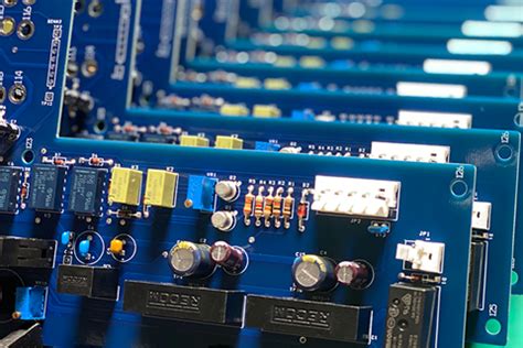
Challenges And Solutions In HDI PCB Assembly
The assembly of High-Density Interconnect (HDI) printed circuit boards (PCBs) presents a unique set of challenges that require innovative solutions to ensure optimal performance and reliability. As electronic devices continue to shrink in size while increasing in functionality, the demand for HDI PCBs has surged. These advanced circuit boards are characterized by their higher wiring density per unit area, achieved through finer lines and spaces, smaller vias, and capture pads. However, the complexity inherent in HDI PCB assembly necessitates a thorough understanding of the challenges involved and the strategies to overcome them.
One of the primary challenges in HDI PCB assembly is the precise alignment required for the microvias, which are significantly smaller than traditional vias.
These microvias are crucial for connecting the multiple layers of the PCB, and any misalignment can lead to electrical failures. To address this, manufacturers employ advanced laser drilling techniques and utilize sophisticated imaging systems to ensure accurate placement. Additionally, implementing automated optical inspection (AOI) systems can help detect alignment issues early in the production process, thereby reducing the risk of defects.
Another significant challenge is the management of thermal stresses during the assembly process.
HDI PCBs often incorporate a variety of materials with different thermal expansion coefficients, which can lead to warping or delamination under high-temperature conditions. To mitigate these risks, manufacturers must carefully select materials that are compatible in terms of thermal properties. Furthermore, employing controlled reflow soldering processes can help manage heat distribution across the board, minimizing the potential for thermal-induced damage.
The miniaturization of components on HDI PCBs also poses a challenge in terms of soldering.
The reduced size of pads and the close proximity of components increase the likelihood of solder bridging and insufficient solder joints. To address this, manufacturers can utilize precision stencil printing techniques and employ solder pastes with appropriate viscosity and particle size. Additionally, the use of advanced reflow ovens with precise temperature control can ensure that soldering is conducted within optimal parameters, reducing the risk of defects.
Signal integrity is another critical concern in HDI PCB assembly.
As the density of interconnections increases, so does the potential for signal interference and crosstalk. To combat this, designers must carefully plan the layout of the PCB, incorporating techniques such as differential signaling and controlled impedance routing. Moreover, the use of high-quality dielectric materials can help maintain signal integrity by reducing signal loss and minimizing electromagnetic interference.
Finally, the inspection and testing of HDI PCBs present their own set of challenges due to the complexity and density of the boards.
Traditional testing methods may not be sufficient to identify all potential issues. Therefore, manufacturers often employ a combination of in-circuit testing (ICT) and functional testing to ensure comprehensive coverage. Additionally, the use of X-ray inspection systems can provide valuable insights into the internal structure of the PCB, allowing for the detection of hidden defects such as voids or misaligned vias.
In conclusion, while the assembly of HDI PCBs is fraught with challenges, a combination of advanced technologies and meticulous planning can effectively address these issues. By leveraging precision manufacturing techniques, careful material selection, and comprehensive testing protocols, manufacturers can produce HDI PCBs that meet the demanding requirements of modern electronic devices. As technology continues to evolve, ongoing innovation in HDI PCB assembly will be essential to keep pace with the ever-increasing demands of the electronics industry.