Hdi pcb via
Understanding HDI PCB Via Types: Microvias, Blind Vias, and Buried Vias
High-Density Interconnect (HDI) technology has revolutionized the printed circuit board (PCB) industry by enabling the design of more compact and efficient electronic devices. A critical aspect of HDI PCBs is the use of various via types, which facilitate electrical connections between different layers of the board. Understanding the distinctions between microvias, blind vias, and buried vias is essential for engineers and designers aiming to optimize the performance and reliability of their electronic products.
Microvias are a defining feature of HDI PCBs, characterized by their small diameter, typically less than 150 micrometers.
These vias are drilled using laser technology, allowing for precise and accurate placement. The primary advantage of microvias is their ability to connect only the outermost layers of a PCB, which significantly reduces the space required for routing. This reduction in space is crucial for modern electronic devices that demand high functionality within a limited form factor. Moreover, microvias contribute to improved signal integrity by minimizing the length of the signal path, thereby reducing the potential for signal loss and interference.
Transitioning to blind vias, these are another vital component in the HDI PCB landscape.
Unlike microvias, blind vias extend from an outer layer of the PCB to one or more inner layers but do not pass through the entire board. This characteristic makes blind vias particularly useful for connecting surface-mounted components to internal layers without occupying valuable real estate on the opposite side of the board. The use of blind vias allows for more complex layer stacking and routing, which is essential for high-performance applications where space is at a premium. Additionally, blind vias can help in reducing the overall weight of the PCB, a critical factor in applications such as aerospace and portable electronics.
In contrast, buried vias are located entirely within the internal layers of the PCB, making them invisible from the outer surfaces.
These vias connect two or more inner layers without reaching the external layers, thus providing a means to route signals internally without affecting the surface layout. Buried vias are particularly advantageous in multi-layer PCBs where internal routing is necessary to maintain a clean and efficient surface design. By utilizing buried vias, designers can achieve higher layer counts and more intricate routing schemes, which are often required in advanced electronic systems.
The integration of these via types in HDI PCBs offers numerous benefits, including increased circuit density, enhanced electrical performance, and greater design flexibility.
However, it is important to consider the manufacturing complexities and cost implications associated with each via type. For instance, the precision required for laser drilling microvias can increase production costs, while the additional steps needed to create blind and buried vias may extend manufacturing time. Therefore, a careful balance must be struck between the desired performance characteristics and the practical constraints of production.
In conclusion, the strategic use of microvias, blind vias, and buried vias in HDI PCBs is instrumental in meeting the demands of modern electronic devices. By understanding the unique properties and applications of each via type, engineers and designers can make informed decisions that enhance the functionality and efficiency of their products. As technology continues to advance, the role of these via types will undoubtedly become even more critical in the development of next-generation electronic systems.
The Role of HDI PCB Vias in Miniaturization and High-Density Interconnects
High-Density Interconnect (HDI) printed circuit boards (PCBs) have become a cornerstone in the advancement of modern electronics, primarily due to their ability to support miniaturization and high-density interconnects. At the heart of this technological evolution are HDI PCB vias, which play a crucial role in enhancing the performance and functionality of electronic devices. As electronic devices continue to shrink in size while increasing in complexity, the demand for efficient and reliable interconnect solutions has never been greater. HDI PCB vias address this demand by enabling more connections in a smaller area, thus facilitating the miniaturization of electronic components.
To understand the significance of HDI PCB vias, it is essential to first comprehend what vias are.
Vias are conductive pathways that allow electrical connections between different layers of a PCB. In traditional PCBs, these vias are typically through-hole vias, which extend from the top to the bottom layer of the board. However, as the need for more compact and efficient designs has grown, the limitations of through-hole vias have become apparent. This is where HDI PCB vias come into play, offering a more sophisticated solution.
HDI PCB vias are categorized into several types, including microvias, blind vias, and buried vias.
Microvias are small-diameter vias that connect adjacent layers and are typically formed using laser drilling. Their small size allows for a higher density of connections, which is essential for modern electronic devices that require complex circuitry in a limited space. Blind vias, on the other hand, connect an outer layer to one or more inner layers but do not extend through the entire board.
This type of via is particularly useful in HDI designs as it maximizes the available space on the outer layers for component placement. Buried vias are located entirely within the inner layers of the PCB, providing connections between these layers without affecting the outer surfaces. The combination of these via types in HDI PCBs allows for a more efficient use of space and resources, leading to smaller, lighter, and more powerful electronic devices.
The role of HDI PCB vias in miniaturization is further underscored by their impact on signal integrity and performance.
As electronic devices become more compact, the proximity of components can lead to issues such as signal interference and crosstalk. HDI PCB vias help mitigate these issues by providing shorter and more direct pathways for electrical signals, thereby reducing the potential for interference. This is particularly important in high-frequency applications where signal integrity is paramount.
Moreover, the use of HDI PCB vias contributes to the overall reliability and durability of electronic devices.
By reducing the number of through-hole vias, which can weaken the structural integrity of the board, HDI designs enhance the mechanical strength of the PCB. This is crucial for devices that are subject to physical stress or harsh environmental conditions.
In conclusion, HDI PCB vias are integral to the ongoing trend of miniaturization and high-density interconnects in the electronics industry. By enabling more efficient use of space, improving signal integrity, and enhancing the reliability of electronic devices, these vias are paving the way for the next generation of technology. As the demand for smaller, faster, and more powerful devices continues to grow, the role of HDI PCB vias will undoubtedly become even more significant in shaping the future of electronics.
Design Considerations for HDI PCB Vias: Ensuring Reliability and Performance
In the realm of modern electronics, High-Density Interconnect (HDI) printed circuit boards (PCBs) have become a cornerstone of advanced design, offering enhanced performance and miniaturization capabilities. A critical aspect of HDI PCB design is the implementation of vias, which are essential for establishing electrical connections between different layers of the board. As designers strive to meet the increasing demands for reliability and performance, understanding the design considerations for HDI PCB vias is paramount.
To begin with, the choice of via type plays a significant role in the overall performance of an HDI PCB.
There are several types of vias, including through-hole vias, blind vias, and buried vias, each serving distinct purposes. Through-hole vias extend through the entire board, while blind vias connect an outer layer to one or more inner layers without passing through the entire board. Buried vias, on the other hand, connect internal layers without reaching the outer surfaces. The selection of via type depends on factors such as board thickness, layer count, and the specific electrical requirements of the design. For instance, blind and buried vias are often preferred in HDI designs due to their ability to save space and reduce signal path lengths, thereby enhancing signal integrity.
Moreover, the size and aspect ratio of vias are crucial considerations that directly impact the reliability of the PCB.
Smaller vias are advantageous in HDI designs as they allow for higher component density and more efficient use of board space. However, reducing via size can also introduce challenges related to manufacturing precision and mechanical strength. The aspect ratio, defined as the ratio of the via’s depth to its diameter, must be carefully managed to ensure reliable plating and structural integrity. A high aspect ratio can lead to difficulties in plating uniformity, potentially resulting in weak or incomplete connections. Therefore, designers must strike a balance between miniaturization and manufacturability to achieve optimal results.
Transitioning to the topic of via placement, strategic positioning is essential for minimizing signal interference and optimizing electrical performance.
Vias should be placed to minimize the length of signal paths, thereby reducing inductance and potential signal degradation. Additionally, careful consideration must be given to the thermal management of the PCB. Vias can serve as thermal conduits, aiding in the dissipation of heat generated by high-power components. Proper thermal via placement can significantly enhance the thermal performance of the board, ensuring that components operate within their specified temperature ranges.
Furthermore, the choice of materials used in via construction is another critical factor influencing the reliability and performance of HDI PCBs.
The selection of suitable dielectric materials and copper plating processes can affect the electrical characteristics and mechanical stability of the vias. High-quality materials and precise manufacturing processes are essential to prevent issues such as via cracking, delamination, or electrical failure, which can compromise the functionality of the entire PCB.
In conclusion, the design considerations for HDI PCB vias are multifaceted, encompassing via type selection, size and aspect ratio management, strategic placement, and material choice. By carefully addressing these factors, designers can ensure that their HDI PCBs meet the stringent demands of modern electronic applications, delivering both reliability and high performance. As technology continues to advance, the importance of meticulous via design in HDI PCBs will only grow, underscoring the need for ongoing innovation and expertise in this critical area of electronics design.

Manufacturing Challenges and Solutions for HDI PCB Via Implementation
High-Density Interconnect (HDI) printed circuit boards (PCBs) have become a cornerstone in the advancement of modern electronics, offering enhanced performance and miniaturization capabilities. However, the implementation of vias in HDI PCBs presents a unique set of manufacturing challenges that require innovative solutions. Understanding these challenges and the corresponding solutions is crucial for manufacturers aiming to optimize the production process and ensure the reliability of the final product.
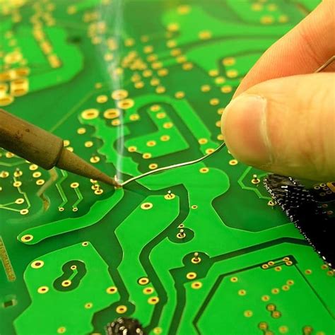
One of the primary challenges in HDI PCB via implementation is the precision required in drilling microvias.
Unlike traditional PCBs, HDI boards often utilize microvias, which are significantly smaller in diameter. This necessitates the use of advanced laser drilling techniques, as mechanical drilling methods are inadequate for such fine features. Laser drilling, while effective, introduces its own set of challenges, including the need for precise control over laser parameters to prevent damage to the substrate and ensure clean, accurate holes. Manufacturers must invest in high-quality laser equipment and develop stringent process controls to mitigate these issues.
In addition to drilling, the plating of microvias poses another significant challenge.
Ensuring reliable electrical connections through these tiny vias requires uniform copper plating, which can be difficult to achieve due to the aspect ratio of the vias. Traditional electroplating methods may not provide the necessary uniformity, leading to potential reliability issues such as voids or insufficient copper thickness. To address this, manufacturers have turned to advanced plating techniques, such as direct metallization and pulse plating, which offer improved control over the deposition process and result in more consistent plating quality.
Moreover, the integration of HDI vias into multilayer PCB designs adds complexity to the manufacturing process.
The need to align multiple layers with high precision is critical, as any misalignment can lead to connectivity issues and compromised board performance. This challenge is exacerbated by the shrinking tolerances associated with HDI designs. To overcome this, manufacturers employ advanced registration systems and employ techniques such as optical alignment to ensure precise layer stacking. Additionally, the use of automated optical inspection (AOI) systems helps in early detection of alignment issues, allowing for corrective actions before the final assembly.
Thermal management is another area where HDI PCB via implementation presents challenges.
The increased density of components and vias can lead to higher thermal loads, which, if not managed properly, can affect the performance and longevity of the PCB. Manufacturers must carefully consider the thermal properties of materials used in HDI PCBs and may need to incorporate thermal vias or other heat dissipation techniques to effectively manage heat.
Finally, cost considerations cannot be overlooked. The advanced technologies and materials required for HDI PCB via implementation can lead to higher production costs. Manufacturers must balance the need for cutting-edge capabilities with cost-effectiveness, often necessitating a strategic approach to material selection and process optimization. By leveraging economies of scale and continuous process improvements, manufacturers can mitigate some of these cost challenges.
In conclusion, while the implementation of vias in HDI PCBs presents several manufacturing challenges, advancements in technology and process optimization offer viable solutions. By addressing issues related to drilling, plating, alignment, thermal management, and cost, manufacturers can successfully produce high-quality HDI PCBs that meet the demands of modern electronic applications.