Hdi vs standard pcb
Advantages Of HDI Over Standard PCB
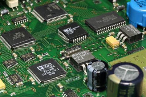
In the realm of electronics manufacturing, the choice between High-Density Interconnect (HDI) and standard Printed Circuit Boards (PCBs) is pivotal, as it significantly influences the performance, size, and functionality of electronic devices. HDI technology, characterized by its higher wiring density per unit area, offers several advantages over traditional PCBs, making it a preferred choice for modern electronic applications.
To begin with, one of the most notable advantages of HDI over standard PCBs is the ability to accommodate more components in a smaller area.
This is achieved through the use of finer lines and spaces, smaller vias, and capture pads, which collectively allow for a more compact design. Consequently, HDI boards are ideal for applications where space is at a premium, such as in smartphones, tablets, and other portable devices. The miniaturization of components not only enhances the portability of devices but also contributes to the overall reduction in weight, which is a critical factor in consumer electronics.
Moreover, HDI technology significantly improves the electrical performance of the circuit board.
The shorter distance between components reduces signal loss and enhances signal integrity, which is crucial for high-speed applications. This improvement in performance is particularly beneficial in advanced computing and telecommunications, where rapid data transmission and processing are essential. Additionally, the use of microvias in HDI boards reduces the parasitic inductance and capacitance, further enhancing the board’s electrical characteristics.
Another advantage of HDI over standard PCBs is the increased reliability and durability of the final product.
The advanced materials and manufacturing processes used in HDI production result in boards that are more robust and less prone to mechanical failure. This is particularly important in applications where the device is subject to harsh environmental conditions or mechanical stress. Furthermore, the improved thermal management capabilities of HDI boards, due to their efficient heat dissipation properties, contribute to the longevity and reliability of electronic devices.
In addition to these technical benefits, HDI technology also offers economic advantages.
Although the initial cost of HDI production may be higher due to the complexity of the manufacturing process, the overall cost-effectiveness is realized through the reduction in material usage and the potential for higher yields. The ability to integrate more functionality into a single board reduces the need for additional components and interconnections, leading to cost savings in both materials and assembly. This economic efficiency is particularly advantageous in large-scale production, where even small savings per unit can result in significant financial benefits.
Furthermore, the versatility of HDI technology allows for greater design flexibility, enabling engineers to create innovative and complex designs that were previously unattainable with standard PCBs.
This flexibility is crucial in the rapidly evolving electronics industry, where the demand for more sophisticated and multifunctional devices continues to grow. The ability to quickly adapt to new design requirements and incorporate cutting-edge technologies gives manufacturers a competitive edge in the market.
In conclusion, the advantages of HDI over standard PCBs are manifold, encompassing improvements in size, performance, reliability, cost-effectiveness, and design flexibility. As the demand for more compact, efficient, and reliable electronic devices continues to rise, HDI technology is poised to play an increasingly important role in the future of electronics manufacturing.

Cost Comparison: HDI Vs Standard PCB
In the realm of electronics manufacturing, the choice between High-Density Interconnect (HDI) and standard Printed Circuit Boards (PCBs) is a critical decision that can significantly impact both the performance and cost of the final product. Understanding the cost implications of each option is essential for manufacturers aiming to optimize their production processes while maintaining high-quality standards. As we delve into the cost comparison between HDI and standard PCBs, it is important to consider various factors that contribute to the overall expenses associated with each type.
To begin with, HDI PCBs are known for their advanced technology, which allows for a higher density of components on a smaller board.
This is achieved through the use of microvias, finer lines, and spaces, as well as multiple layers. Consequently, the manufacturing process for HDI PCBs is more complex and requires specialized equipment and expertise. This complexity often translates into higher initial production costs compared to standard PCBs. The need for precision in the fabrication of HDI boards means that manufacturers must invest in state-of-the-art technology and skilled labor, both of which contribute to the increased cost.
In contrast, standard PCBs are generally less expensive to produce due to their simpler design and manufacturing process.
They typically involve fewer layers and larger vias, which do not require the same level of precision as HDI boards. As a result, the equipment and labor costs associated with standard PCB production are lower. This makes standard PCBs a more cost-effective option for projects where space and performance constraints are not as critical.
However, it is crucial to consider the long-term cost implications of choosing between HDI and standard PCBs. .
While HDI boards may have higher upfront costs, they can offer significant savings in terms of space and weight reduction. This is particularly beneficial in industries such as aerospace and consumer electronics, where minimizing size and weight is paramount. By enabling more compact designs, HDI PCBs can lead to reduced material costs and potentially lower shipping expenses, offsetting their initial higher production costs.
Moreover, the enhanced performance capabilities of HDI PCBs can result in cost savings over the product’s lifecycle.
The ability to incorporate more components and achieve higher functionality on a single board can reduce the need for additional PCBs or components, thereby lowering assembly and material costs. Additionally, the improved reliability and performance of HDI boards can lead to fewer failures and reduced maintenance costs, further enhancing their cost-effectiveness in the long run.
On the other hand, for applications where the advanced features of HDI PCBs are not necessary, standard PCBs remain a viable and economical choice.
Their lower production costs make them suitable for high-volume production runs where cost efficiency is a priority. Furthermore, the widespread availability of standard PCB manufacturing facilities ensures competitive pricing and shorter lead times, which can be advantageous for projects with tight deadlines.
In conclusion, the cost comparison between HDI and standard PCBs is not straightforward and depends on various factors, including the specific requirements of the project and the intended application. While HDI PCBs may entail higher initial costs, their potential for space savings, enhanced performance, and long-term cost benefits make them an attractive option for certain applications. Conversely, standard PCBs offer a more economical solution for projects where advanced features are not essential. Ultimately, manufacturers must carefully evaluate their needs and priorities to make an informed decision that balances cost with performance and functionality.

Design Considerations For HDI And Standard PCB
When embarking on the journey of designing printed circuit boards (PCBs), engineers and designers are often faced with the decision of choosing between High-Density Interconnect (HDI) PCBs and standard PCBs. This choice is pivotal, as it influences not only the performance and functionality of the final product but also its cost and manufacturability. Understanding the design considerations for both HDI and standard PCBs is essential for making an informed decision that aligns with the specific requirements of a project.
To begin with, HDI PCBs are characterized by their ability to accommodate a higher density of components and interconnections within a smaller footprint.
This is achieved through the use of advanced technologies such as microvias, blind and buried vias, and finer trace widths and spaces. Consequently, HDI PCBs are particularly advantageous in applications where space is at a premium, such as in smartphones, tablets, and other compact electronic devices. The ability to integrate more functionality into a smaller area allows for the creation of more sophisticated and feature-rich products.
In contrast, standard PCBs, which utilize through-hole vias and have larger trace widths and spaces, are typically employed in applications where space constraints are less of a concern. These boards are often used in larger electronic devices or in applications where cost is a significant factor. Standard PCBs are generally easier and less expensive to manufacture, making them a viable option for projects with budgetary limitations or where the complexity of the circuitry does not necessitate the advanced capabilities of HDI technology.
Transitioning from the basic characteristics of each type, it is important to consider the implications of these differences on the design process.
HDI PCBs require a more meticulous design approach due to their complexity. Designers must carefully plan the placement of components and the routing of traces to ensure signal integrity and minimize electromagnetic interference. The use of microvias and other advanced features necessitates precise design tools and expertise, which can increase the time and cost associated with the design phase. However, the benefits of HDI technology, such as improved electrical performance and reduced weight, often justify these additional efforts.
On the other hand, the design process for standard PCBs is generally more straightforward.
The larger features and simpler construction allow for easier routing and placement of components. This can result in shorter design cycles and reduced costs, making standard PCBs an attractive option for projects with less demanding performance requirements. However, it is crucial to recognize that the limitations in density and performance may restrict the potential applications of standard PCBs, particularly in cutting-edge technologies.
In conclusion, the decision between HDI and standard PCBs hinges on a careful evaluation of the specific needs and constraints of a project. While HDI PCBs offer significant advantages in terms of miniaturization and performance, they come with increased complexity and cost. Conversely, standard PCBs provide a more economical and simpler solution but may fall short in applications requiring high density and advanced functionality. By thoroughly understanding the design considerations associated with each type, engineers and designers can make informed choices that optimize the balance between performance, cost, and manufacturability, ultimately leading to the successful realization of their electronic products.
Applications Of HDI And Standard PCB In Modern Electronics
In the rapidly evolving landscape of modern electronics, the choice between High-Density Interconnect (HDI) and standard Printed Circuit Boards (PCBs) plays a crucial role in determining the performance, size, and functionality of electronic devices. As technology advances, the demand for more compact, efficient, and powerful electronic components has led to the increased adoption of HDI PCBs in various applications. However, standard PCBs continue to hold their ground in numerous sectors due to their cost-effectiveness and reliability. Understanding the applications of both HDI and standard PCBs is essential for making informed decisions in electronic design and manufacturing.
HDI PCBs are characterized by their higher wiring density per unit area, achieved through the use of finer lines and spaces, smaller vias, and capture pads.
This allows for more components to be placed on a smaller board, making HDI PCBs ideal for applications where space is at a premium. Consequently, they are extensively used in the production of smartphones, tablets, and other portable devices. The compact nature of HDI PCBs enables manufacturers to pack more functionality into smaller devices, meeting consumer demand for sleek and lightweight electronics. Moreover, HDI technology supports advanced features such as high-speed signal transmission and improved thermal management, which are critical in high-performance computing and telecommunications equipment.
In contrast, standard PCBs are typically employed in applications where size constraints are less stringent, and cost considerations are paramount.
These boards are widely used in consumer electronics, automotive systems, and industrial machinery, where their robustness and lower production costs offer significant advantages. Standard PCBs are well-suited for products that do not require the miniaturization capabilities of HDI technology, such as household appliances and larger electronic devices. Additionally, the simpler design and manufacturing processes associated with standard PCBs often result in shorter lead times, making them a practical choice for projects with tight deadlines.
Despite their differences, both HDI and standard PCBs share common ground in certain applications.
For instance, in the realm of medical devices, both types of PCBs are utilized depending on the specific requirements of the device. HDI PCBs are often chosen for wearable medical devices and implantable technologies due to their compact size and ability to support complex functionalities. On the other hand, standard PCBs are frequently used in larger medical equipment, such as imaging systems and diagnostic machines, where their durability and cost-effectiveness are advantageous.
As the Internet of Things (IoT) continues to expand, the demand for both HDI and standard PCBs is expected to grow. IoT devices, ranging from smart home appliances to industrial sensors, require a diverse array of PCB solutions to accommodate varying design and performance needs. HDI PCBs are particularly beneficial in IoT applications that require miniaturization and high-speed data processing, while standard PCBs offer a reliable and economical option for less complex devices.
In conclusion, the choice between HDI and standard PCBs is largely dictated by the specific requirements of the application at hand. HDI PCBs excel in scenarios where space, performance, and advanced features are critical, while standard PCBs provide a cost-effective and reliable solution for a wide range of electronic products. As technology continues to advance, the complementary roles of HDI and standard PCBs will remain integral to the development of innovative electronic devices across various industries.