High-Current PCB Design: A Pitfall Avoidance Guide
Introduction
Printed Circuit Boards (PCBs) designed for high-current applications require careful consideration of thermal management, trace width, material selection, and component placement. Unlike low-power PCBs, high-current designs face challenges such as excessive heat generation, voltage drops, and potential failure due to inadequate current handling.
This guide explores common pitfalls in high-current PCB design and provides actionable strategies to avoid them, ensuring reliability, efficiency, and longevity.
1. Understanding High-Current PCB Design Challenges
High-current PCBs (typically handling currents above 10A) must address:
- Heat dissipation – Excessive current generates heat, leading to thermal stress.
- Voltage drop – Long or thin traces increase resistance, reducing efficiency.
- Electromagnetic interference (EMI) – High currents can induce noise in adjacent circuits.
- Mechanical stress – Thermal expansion and high currents can weaken solder joints.
Avoiding these issues requires careful planning in layout, material selection, and component choice.
2. Common Pitfalls and How to Avoid Them
Pitfall #1: Inadequate Trace Width and Thickness
Issue: Thin or narrow traces overheat and fail under high current due to excessive resistance.
Solution:
- Use trace width calculators (e.g., IPC-2152 standard) to determine optimal dimensions.
- Wider traces reduce resistance and heat buildup.
- Increase copper weight (e.g., 2 oz/ft² or higher) to improve current capacity.
- For extreme currents, use bus bars or external conductors instead of relying solely on PCB traces.
Pitfall #2: Poor Thermal Management
Issue: High currents generate heat, leading to component failure or delamination.
Solution:
- Use thermal vias to conduct heat away from critical components.
- Incorporate heatsinks or thermal pads for power components (e.g., MOSFETs, regulators).
- Select high-Tg (glass transition temperature) materials (e.g., FR4 with Tg > 170°C).
- Ensure proper airflow in the enclosure or use forced cooling (fans, liquid cooling).
Pitfall #3: Incorrect PCB Material Selection
Issue: Standard FR4 may not handle high temperatures or current densities.
Solution:
- For extreme conditions, use metal-core PCBs (MCPCBs) or ceramic substrates for better heat dissipation.
- Choose high-current laminates like polyimide or Rogers materials for improved thermal performance.
Pitfall #4: Neglecting Current Distribution in Multi-Layer PCBs
Issue: Uneven current distribution leads to localized heating and failure.
Solution:
- Use multiple layers with thick copper planes to distribute current evenly.
- Implement symmetrical power and ground planes to minimize loop inductance.
- Avoid sharp bends in traces—use curved or 45° angles to reduce current crowding.
Pitfall #5: Inadequate Via Design
Issue: High-current vias can overheat or crack due to thermal cycling.
Solution:
- Use multiple vias in parallel to share current load.
- Prefer tented vias (covered with solder mask) to prevent solder wicking.
- For very high currents, use plugged vias (filled with conductive epoxy).
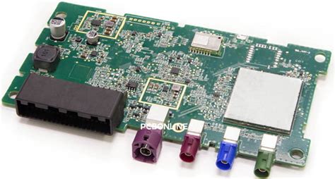
Pitfall #6: Poor Component Placement and Routing
Issue: Long traces increase resistance and inductance, reducing efficiency.
Solution:
- Place high-current components (e.g., inductors, power FETs) close together to minimize trace length.
- Use Kelvin connections for precise current sensing.
- Separate high-current and low-current paths to avoid noise coupling.
Pitfall #7: Ignoring EMI and Crosstalk
Issue: High-current switching (e.g., in motor drivers or DC-DC converters) generates EMI.
Solution:
- Use ground planes to shield sensitive signals.
- Implement snubber circuits to suppress voltage spikes.
- Keep high-frequency switching traces short and away from analog signals.
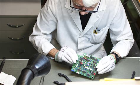
Pitfall #8: Underestimating Solder Joint Reliability
Issue: High currents can weaken solder joints over time.
Solution:
- Use thick solder pads and reinforced plating for high-current connections.
- Consider wave soldering or selective soldering for high-power components.
- Apply conformal coating to protect against environmental stress.
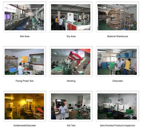
Pitfall #9: Lack of Proper Testing and Validation
Issue: Undetected design flaws lead to field failures.
Solution:
- Perform thermal imaging to identify hotspots.
- Use 4-wire (Kelvin) measurement for accurate resistance checks.
- Conduct high-current stress tests before full production.
3. Best Practices for High-Current PCB Design
To summarize, follow these best practices:
- Optimize trace width and copper weight based on current requirements.
- Use thermal vias and heatsinks for effective heat dissipation.
- Select appropriate PCB materials (e.g., MCPCBs for high-power applications).
- Distribute current evenly with multiple layers and symmetrical planes.
- Strengthen vias and solder joints to handle thermal stress.
- Minimize EMI with proper grounding and shielding.
- Test rigorously under real-world conditions before deployment.
Conclusion
High-current PCB design demands meticulous attention to thermal, electrical, and mechanical factors. By avoiding common pitfalls—such as inadequate trace sizing, poor thermal management, and improper via design—engineers can create robust, high-performance PCBs capable of handling demanding applications.
Implementing these guidelines will enhance reliability, efficiency, and longevity, ensuring that your high-current PCB performs optimally under real-world conditions.