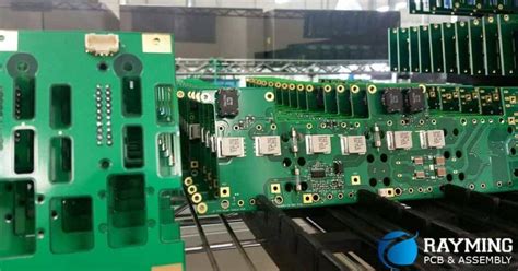
High frequency digital pcb design
Signal Integrity Challenges in High Frequency PCB Design
In the realm of high frequency digital PCB design, signal integrity emerges as a pivotal concern, demanding meticulous attention to detail and a comprehensive understanding of electromagnetic principles. As digital circuits operate at increasingly higher frequencies, the challenges associated with maintaining signal integrity become more pronounced. This is primarily due to the fact that at high frequencies, the behavior of signals deviates significantly from the predictable patterns observed at lower frequencies. Consequently, designers must navigate a complex landscape of potential issues that can compromise the performance and reliability of the final product.
One of the foremost challenges in high frequency PCB design is the management of signal reflections.
At high frequencies, the wavelength of signals becomes comparable to the physical dimensions of the PCB traces. This can lead to impedance mismatches, which in turn cause signal reflections. These reflections can interfere with the original signal, leading to distortion and potential data loss. To mitigate this, designers often employ techniques such as impedance matching and the use of termination resistors. By carefully designing the trace geometry and selecting appropriate materials, it is possible to minimize these reflections and preserve signal integrity.
In addition to reflections, crosstalk is another significant concern in high frequency PCB design.
Crosstalk occurs when a signal on one trace inadvertently couples with an adjacent trace, causing unwanted interference. This phenomenon is exacerbated at high frequencies due to the increased electromagnetic field strength. To address crosstalk, designers can increase the spacing between traces, use differential signaling, or implement shielding techniques. These strategies help to isolate signals and reduce the likelihood of interference, thereby enhancing the overall performance of the PCB.
Moreover, power integrity is closely linked to signal integrity in high frequency designs.
Fluctuations in the power supply can introduce noise into the system, which can degrade signal quality. To ensure stable power delivery, designers must focus on optimizing the power distribution network (PDN). This involves careful placement of decoupling capacitors, strategic routing of power and ground planes, and minimizing the loop area of power delivery paths. By maintaining a robust PDN, the impact of power-related noise on signal integrity can be significantly reduced.
Furthermore, electromagnetic interference (EMI) poses a formidable challenge in high frequency PCB design.
EMI can originate from both internal and external sources, and it can disrupt the operation of sensitive components. To combat EMI, designers often employ a combination of grounding techniques, shielding, and filtering. Ground planes can be used to provide a low-impedance path for return currents, while shielding can prevent external electromagnetic fields from penetrating the PCB. Additionally, filters can be used to suppress unwanted frequency components, ensuring that only the desired signals are transmitted.
In conclusion, maintaining signal integrity in high frequency digital PCB design is a multifaceted challenge that requires a holistic approach. By addressing issues such as signal reflections, crosstalk, power integrity, and electromagnetic interference, designers can create PCBs that perform reliably in demanding environments. As technology continues to advance and operating frequencies increase, the importance of signal integrity will only grow, underscoring the need for innovative design strategies and a deep understanding of electromagnetic principles. Through careful planning and execution, it is possible to overcome these challenges and achieve optimal performance in high frequency digital systems.

Best Practices for Layer Stackup in High Frequency PCBs
In the realm of high frequency digital PCB design, the layer stackup plays a pivotal role in determining the performance and reliability of the final product. As electronic devices continue to shrink in size while increasing in functionality, the demand for high frequency PCBs has surged. Consequently, understanding the best practices for layer stackup becomes essential for engineers and designers aiming to optimize signal integrity and minimize electromagnetic interference.
To begin with, the selection of materials is a fundamental consideration in high frequency PCB design.
The dielectric material used between the layers significantly impacts the board’s electrical properties. Materials with low dielectric constant (Dk) and low dissipation factor (Df) are preferred, as they reduce signal loss and ensure faster signal propagation. Furthermore, the choice of copper thickness is crucial; thinner copper layers are often favored in high frequency applications to minimize skin effect, which can lead to increased resistance and signal attenuation at higher frequencies.
Transitioning to the configuration of the layer stackup, it is imperative to maintain a symmetrical structure.
A balanced stackup not only enhances mechanical stability but also aids in reducing warpage during the manufacturing process. Typically, a multi-layer PCB will include a combination of signal, power, and ground layers. The arrangement of these layers should be carefully planned to ensure effective isolation of high frequency signals from power and ground planes, thereby minimizing crosstalk and electromagnetic interference.
Moreover, the placement of ground planes is a critical aspect of layer stackup design.
Ground planes should be positioned adjacent to signal layers to provide a return path for high frequency signals. This proximity helps in reducing loop inductance and maintaining signal integrity. Additionally, it is advisable to use multiple ground planes in the stackup, as they can serve as effective shields against electromagnetic interference, further enhancing the board’s performance.
Another best practice involves the strategic use of power planes.
Power planes should be placed close to ground planes to create a low-inductance power distribution network. This configuration not only stabilizes the power supply but also reduces the potential for noise coupling between power and signal layers. Furthermore, incorporating decoupling capacitors between power and ground planes can help in filtering out high frequency noise, ensuring a clean power supply to the active components.
As we delve deeper into the intricacies of layer stackup, the importance of controlled impedance cannot be overstated.
High frequency signals are particularly sensitive to impedance mismatches, which can lead to signal reflections and degradation. To mitigate this, designers must carefully calculate and control the impedance of signal traces by adjusting trace width, spacing, and the dielectric properties of the materials used. Implementing differential pairs for high-speed signals is another effective strategy, as it helps in maintaining consistent impedance and reducing electromagnetic emissions.
In conclusion, the design of layer stackup in high frequency PCBs is a complex yet critical task that demands meticulous attention to detail. By selecting appropriate materials, maintaining a symmetrical structure, strategically placing ground and power planes, and ensuring controlled impedance, designers can significantly enhance the performance and reliability of high frequency digital PCBs. As technology continues to evolve, adhering to these best practices will remain essential in meeting the ever-increasing demands of modern electronic devices.
Techniques for Minimizing Crosstalk in High Frequency Circuits
In the realm of high frequency digital PCB design, minimizing crosstalk is a critical concern for engineers striving to maintain signal integrity and ensure optimal performance. Crosstalk, the unwanted coupling of signals between adjacent traces, can lead to data corruption, increased error rates, and degraded system performance. As digital circuits operate at increasingly higher frequencies, the potential for crosstalk becomes more pronounced, necessitating the implementation of effective design techniques to mitigate its impact.
One fundamental approach to minimizing crosstalk is through careful trace routing.
By maintaining adequate spacing between signal traces, designers can reduce the capacitive and inductive coupling that contributes to crosstalk. The use of differential signaling, where two complementary signals are routed together, can also be beneficial. This technique not only helps in reducing crosstalk but also enhances noise immunity, as the differential pair can effectively cancel out common-mode noise.
Moreover, the strategic use of ground planes plays a pivotal role in crosstalk reduction.
Ground planes act as a reference point for signals and provide a low-impedance path for return currents, thereby minimizing the loop area and reducing inductive coupling. Ensuring that signal traces are routed close to a continuous ground plane can significantly diminish crosstalk. Additionally, implementing guard traces, which are grounded traces placed between signal lines, can further isolate signals and prevent unwanted coupling.
Transitioning to the topic of signal integrity, the importance of controlled impedance cannot be overstated.
Maintaining consistent impedance along signal paths is crucial for high frequency designs, as impedance mismatches can lead to reflections and increased crosstalk. To achieve controlled impedance, designers must carefully select the PCB materials and stack-up configuration, taking into account the dielectric constant and thickness of each layer. Utilizing simulation tools to model and predict impedance characteristics can aid in optimizing the design for minimal crosstalk.
Furthermore, the role of termination techniques in crosstalk mitigation should be considered.
Properly terminating signal lines with resistors can help absorb reflections and reduce the potential for crosstalk. Series and parallel termination methods, when applied correctly, can effectively dampen signal overshoot and ringing, thereby enhancing signal integrity.
In addition to these techniques, the use of advanced simulation and analysis tools is indispensable in the design process.
Electromagnetic simulation software allows designers to visualize and quantify crosstalk effects, enabling them to make informed decisions about trace routing, layer stack-up, and component placement. By simulating various scenarios, designers can identify potential crosstalk issues early in the design phase and implement corrective measures before fabrication.
Finally, it is essential to consider the impact of via placement on crosstalk.
Vias, which connect traces between different layers of a PCB, can introduce additional inductance and capacitance, exacerbating crosstalk. Minimizing the number of vias and ensuring they are placed strategically can help mitigate these effects. Additionally, using blind or buried vias, which do not pass through all layers of the PCB, can further reduce crosstalk by minimizing the disruption to the ground plane.
In conclusion, minimizing crosstalk in high frequency digital PCB design requires a comprehensive approach that encompasses trace routing, ground plane utilization, controlled impedance, termination techniques, and strategic via placement. By employing these techniques and leveraging advanced simulation tools, designers can effectively mitigate crosstalk, ensuring robust signal integrity and optimal circuit performance. As technology continues to advance, the importance of these design considerations will only grow, underscoring the need for ongoing innovation and adaptation in the field of high frequency digital PCB design.

Material Selection for High Frequency PCB Applications
In the realm of high frequency digital PCB design, the selection of materials plays a pivotal role in determining the performance and reliability of the final product. As electronic devices continue to evolve, operating at increasingly higher frequencies, the demand for materials that can support these frequencies without compromising signal integrity has become more pronounced. Consequently, understanding the properties and implications of various materials is essential for engineers and designers working in this field.
To begin with, one must consider the dielectric constant (Dk) of the substrate material.
The dielectric constant is a measure of a material’s ability to store electrical energy in an electric field. For high frequency applications, it is crucial to select materials with a low and stable dielectric constant. This is because variations in the dielectric constant can lead to signal distortion and impedance mismatches, which are detrimental to the performance of high frequency circuits. Materials such as PTFE (Polytetrafluoroethylene) and certain ceramic-filled laminates are often preferred due to their low dielectric constants and minimal loss characteristics.
In addition to the dielectric constant, the dissipation factor (Df) is another critical parameter to consider.
The dissipation factor indicates the amount of energy lost as heat in the dielectric material. A low dissipation factor is desirable for high frequency applications as it ensures minimal signal loss and heat generation, thereby enhancing the efficiency of the circuit. Advanced materials like Rogers RO4000 series and Taconic RF-35 are known for their low dissipation factors, making them suitable choices for high frequency PCB designs.
Moreover, thermal management is a significant concern in high frequency applications.
As frequencies increase, so does the potential for heat generation, which can adversely affect the performance and longevity of the PCB. Therefore, materials with good thermal conductivity are essential to effectively dissipate heat. Copper-clad laminates with enhanced thermal properties are often employed to address this issue, ensuring that the PCB can operate reliably under high thermal loads.
Furthermore, the coefficient of thermal expansion (CTE) is a vital consideration in material selection.
The CTE measures how much a material expands or contracts with temperature changes. A mismatch in CTE between the substrate and other components, such as copper traces, can lead to mechanical stress and potential failure of the PCB. Selecting materials with a CTE that closely matches that of copper can mitigate these risks, ensuring structural integrity and reliability.
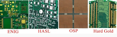
Additionally, the surface finish of the PCB is an important aspect that cannot be overlooked.
The surface finish affects the solderability, corrosion resistance, and overall performance of the PCB. For high frequency applications, finishes such as Electroless Nickel Immersion Gold (ENIG) or Immersion Silver are often preferred due to their excellent conductivity and reliability.
In conclusion, the selection of materials for high frequency digital PCB design is a complex process that requires careful consideration of various factors, including dielectric constant, dissipation factor, thermal management, coefficient of thermal expansion, and surface finish. By understanding and addressing these parameters, designers can ensure that their high frequency PCBs meet the demanding requirements of modern electronic applications, ultimately leading to enhanced performance and reliability. As technology continues to advance, the importance of meticulous material selection in high frequency PCB design will only grow, underscoring its critical role in the success of electronic devices.