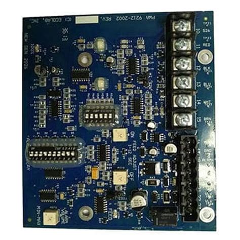
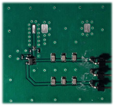
High Frequency PCB Design: Principles, Challenges, and Best Practices
Introduction to High Frequency PCBs
Printed Circuit Boards (PCBs) designed for high frequency applications have become increasingly critical in modern electronics as wireless communication systems, radar, satellite technology, and high-speed digital circuits continue to advance. High frequency PCBs typically operate at frequencies above 500 MHz, with many applications now reaching into the millimeter-wave spectrum (30 GHz and above).
These specialized circuit boards differ significantly from conventional PCBs in their material composition, design considerations, and manufacturing requirements. The unique challenges of high frequency operation demand careful attention to signal integrity, impedance control, and electromagnetic compatibility.
Fundamental Principles of High Frequency PCB Design
Signal Propagation at High Frequencies
At high frequencies, signals no longer behave as simple electrical currents but propagate as electromagnetic waves along transmission lines. This wave nature introduces several critical considerations:
- Skin Effect: As frequency increases, current tends to flow only near the surface of conductors, effectively reducing the usable cross-section and increasing resistance.
- Dielectric Losses: The insulating materials between conductors absorb some of the signal energy, converting it to heat. This loss becomes more significant at higher frequencies.
- Dispersion: Different frequency components of a signal travel at slightly different velocities, potentially distorting signal waveforms.
Transmission Line Theory
Proper high frequency PCB design requires treatment of all conductive paths as transmission lines. Key parameters include:
- Characteristic impedance (typically 50Ω or 75Ω for RF systems)
- Propagation velocity
- Attenuation constant
- Reflection coefficient
Microstrip and stripline are the two most common transmission line configurations used in high frequency PCBs, each with distinct advantages for different applications.

Material Selection for High Frequency PCBs
The choice of substrate material profoundly impacts the performance of high frequency circuits. Key material properties include:
Dielectric Constant (Dk or εᵣ)
The dielectric constant affects signal propagation speed and impedance. Materials with stable Dk across frequency and temperature are essential for predictable performance.
Dissipation Factor (Df or tan δ)
This measures the dielectric loss and becomes increasingly important at higher frequencies. Low-loss materials like PTFE (Teflon) are often preferred despite their higher cost.
Common High Frequency PCB Materials
- FR-4 Modified: Standard FR-4 with improved high frequency characteristics
- PTFE-Based Materials: Rogers RO4000 series, Taconic RF-35
- Ceramic-Filled PTFE: Combining low loss with improved mechanical stability
- Hydrocarbon Ceramics: Lower cost alternative to PTFE with good performance
Critical Design Considerations
Impedance Control
Maintaining consistent characteristic impedance throughout the circuit is paramount. This requires:
- Precise control of trace widths
- Careful management of dielectric thickness
- Consideration of solder mask effects
- Accounting for copper roughness
Crosstalk Mitigation
High frequency signals are particularly susceptible to crosstalk. Design techniques include:
- Appropriate spacing between traces (3x dielectric height is a common rule)
- Use of guard traces or ground vias
- Proper layer stacking with solid reference planes
- Orthogonal routing on adjacent layers
Via Design
Vias present significant challenges at high frequencies due to their discontinuities. Best practices include:
- Minimizing via stubs through back-drilling or blind/buried vias
- Using via fences for shielding
- Proper via pad sizing to minimize capacitance
- Consideration of via inductance in matching networks
Manufacturing Challenges
High frequency PCBs demand tighter tolerances and more specialized processes than conventional boards:
Copper Surface Roughness
Smooth copper surfaces reduce conductor losses at high frequencies. Manufacturers often use rolled copper or special treatments to minimize roughness.
Plating Uniformity
Uneven plating can cause impedance variations. Pulse plating techniques and careful process control help maintain consistency.
Layer-to-Layer Registration
Misalignment between layers affects impedance and can create undesired coupling. Advanced optical alignment systems are typically employed.
Solder Mask Application
Conventional solder masks can negatively impact high frequency performance. Liquid crystal polymer (LCP) coatings or selective masking are often preferred.

Simulation and Verification
Modern high frequency PCB design relies heavily on electromagnetic simulation tools:
3D EM Simulation
Full-wave solvers like HFSS or CST Microwave Studio accurately model complex structures and coupling effects.
Signal Integrity Analysis
Tools like ADS or HyperLynx help predict eye diagrams, jitter, and other signal quality metrics.
Measurement Techniques
Verification typically involves:
- Vector Network Analyzer (VNA) measurements
- Time Domain Reflectometry (TDR)
- Near-field scanning for EMI assessment
Applications of High Frequency PCBs
Wireless Communications
- 5G infrastructure and devices
- Millimeter-wave backhaul
- Small cell antennas
Aerospace and Defense
- Radar systems
- Electronic warfare
- Satellite communications
Automotive
- ADAS radar (77 GHz)
- V2X communication
- In-vehicle networking
Medical
- MRI systems
- Therapeutic and diagnostic equipment
- Wireless implant communication
Future Trends in High Frequency PCB Technology
Higher Frequency Operation
As applications push into the 100+ GHz range, new materials and fabrication techniques will be required.
Integration with Antennas
Antenna-in-package and antenna-on-PCB solutions are becoming more common for compact wireless devices.
Advanced Materials
Developments in low-loss, thermally stable materials continue to push performance boundaries.
Additive Manufacturing
3D printing techniques may enable novel high frequency structures not possible with traditional PCB fabrication.
Conclusion
High frequency PCB design represents a specialized discipline that blends electromagnetic theory, materials science, and precision engineering. As electronic systems continue to operate at higher frequencies and faster data rates, the importance of proper high frequency PCB design only grows. By understanding the fundamental principles, carefully selecting materials, employing rigorous design practices, and utilizing advanced simulation tools, engineers can overcome the challenges posed by high frequency operation and deliver reliable, high-performance electronic systems.
Successful high frequency PCB implementation requires close collaboration between designers, material suppliers, and fabrication houses throughout the development process. With wireless technology becoming ubiquitous across industries, expertise in high frequency PCB design will remain a valuable and sought-after skill in the electronics industry.


